Method for forming opening

a technology of opening and photoresist, which is applied in the direction of semiconductor/solid-state device manufacturing, basic electric elements, electric apparatus, etc., can solve the problems of affecting the quality of the device formed by using the hard mask layer of titanium/titanium nitride, the pattern of the photoresist cannot be accurately transferred onto the material layer, and the inability to provide more effective protection for the material layer

Inactive Publication Date: 2007-03-08
MACRONIX INT CO LTD
View PDF5 Cites 29 Cited by
  • Summary
  • Abstract
  • Description
  • Claims
  • Application Information

AI Technical Summary

Benefits of technology

[0006] Accordingly, at least one objective of the present invention is to provide a method for etching a dielectric layer capable of solving the wafer contamination problem due to the particles generated from the mask layer during the patterning process.

Problems solved by technology

Nevertheless, with respect to those manufacturing process, such as dual damascene process, for forming an opening with a relatively large depth, since the resolution of the photolithography process is decreased with the increase of the thickness of the photoresist, the photoresist cannot provide more effective protection for the material layer.
Therefore, the pattern of the photoresist cannot be accurately transferred onto the material layer.
Therefore, the quality of the device formed by using the titanium / titanium nitride hard mask layer is affected.

Method used


Image

  • Method for forming opening
  • Method for forming opening
  • Method for forming opening

Examples


Embodiment Construction

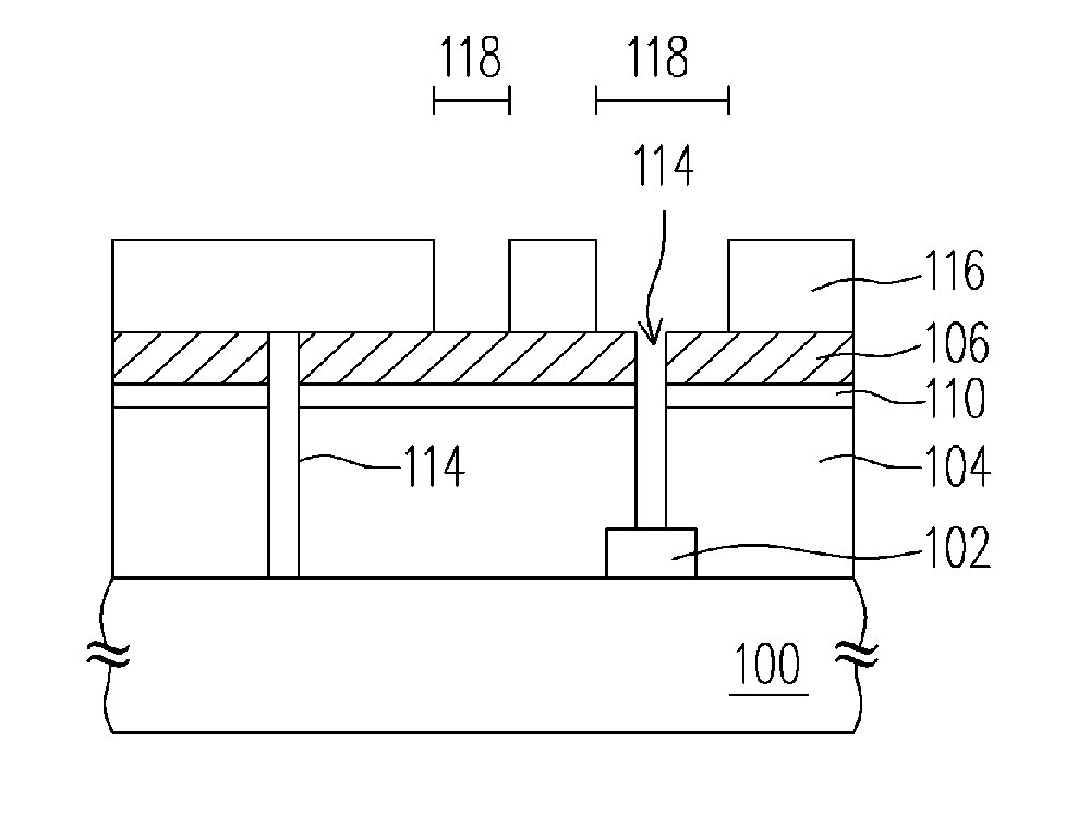
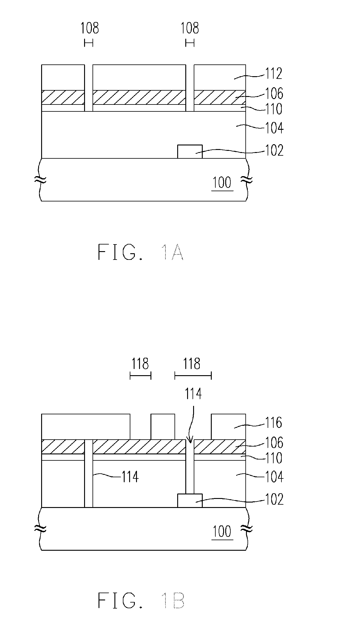
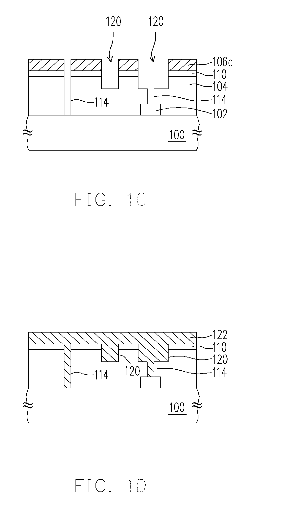
[0019]FIGS. 1A through 1E are cross-sectional views illustrating the method for forming a semiconductor device according to one of the preferred embodiment of the present invention.

[0020] As shown in FIG. 1A, a substrate 100 is provided, wherein the substrate 100 has at least one element structure 102 formed thereon. The substrate 100 can be, for example but not limited to, a silicon substrate. The element structure 102 can be, for example but not limited to, a gate electrode, a conductive wire or a contact plug and the element structure 102 can be made of cobalt silicide or nickel silicide. Further, in one embodiment, the element structure 102 can be a doped region (not shown) formed in the substrate 100.

[0021] Moreover, a dielectric layer 104 is formed over the substrate 100 to cover the element structure 102. The dielectric layer 104 can be, for example but not limited to, made from silicon oxide by performing a chemical vapor deposition.

[0022] In addition, a patterned metal s...


PUM

PropertyMeasurementUnit
conductiveaaaaaaaaaa
dielectricaaaaaaaaaa
thicknessaaaaaaaaaa

Abstract

A method for forming an opening. The method comprises steps of providing a substrate having at least one element structure formed thereon and then forming a dielectric layer over the substrate to cover the element structure. A patterned metal silicide layer is formed on the dielectric layer and then the dielectric layer is etched to form at least one opening by using the patterned metal silicide layer as an etching mask, wherein the opening exposes the corresponding element structure.

Description

BACKGROUND OF THE INVENTION [0001] 1. Field of Invention [0002] The present invention relates to a method for manufacturing a semiconductor device. More particularly, the present invention relates to a method for etching a dielectric layer, a method for forming an opening and a dual damascene process. [0003] 2. Description of Related Art [0004] The photolithography process and etching process play important roles in the semiconductor manufacturing process. The purpose for using the photolithography process is to transfer the patterns from the mask onto a photoresist formed on a material layer. Furthermore, the etching process is used to form a patterned material layer by using the patterned photoresist as an etching mask. Since the photoresist is corroded during the etching process is performed, the thickness of the photoresist is increased in order to prevent the pre-reserved portion of the material layer from being etched through during the etching process. [0005] Nevertheless, wi...

Claims


Application Information

Patent Timeline
Patent Type & Authority Applications(United States)
IPC IPC(8): H01L21/4763H01L21/302
CPCH01L21/76807
Inventor YANG, TA-HUNG
Owner MACRONIX INT CO LTD
Why Eureka
Try Eureka