High current electron beam inspection

Active Publication Date: 2007-03-15
APPL MATERIALS ISRAEL LTD
View PDF8 Cites 75 Cited by
  • Summary
  • Abstract
  • Description
  • Claims
  • Application Information

AI Technical Summary

Benefits of technology

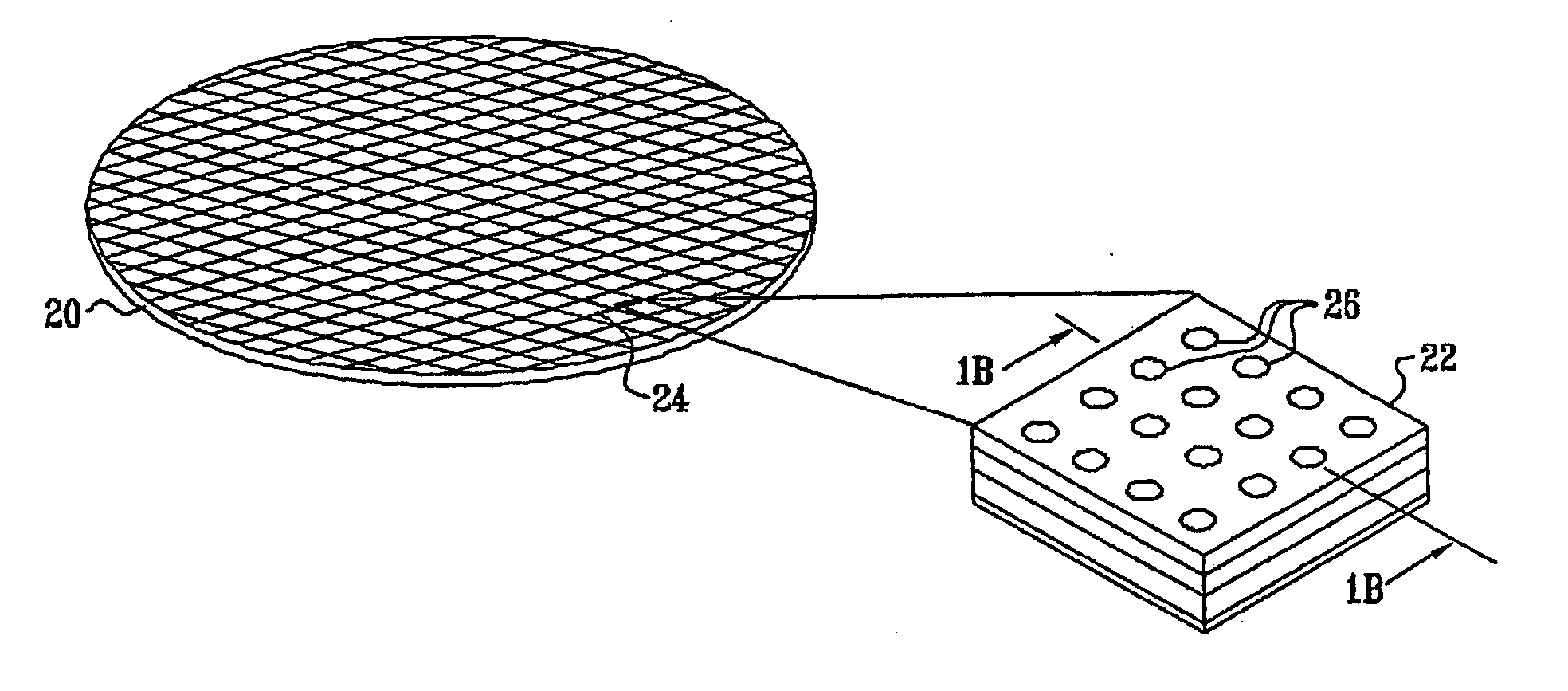
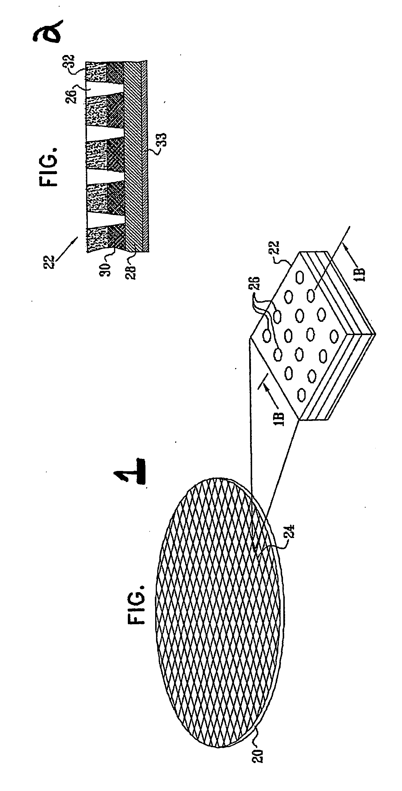
[0009] The invention provides a method for wafer inspection that includes the following steps: (i) receiving a sample having a first layer that is at least partly conductive and a second, dielectric layer formed over the first layer, following production of contact openings in the second layer or even following the generation of contacts; (ii) directing a high current beam of charged pa

Problems solved by technology

If these variations are too large, they impact on device performance and can lead to loss of process yield.
However, HAR imaging has some limitations.
One limitation is that HAR imaging quality of the bottom of holes is significantly limited when the hole bottom is not connected to ground.
Moreover, HA

Method used


Image

  • High current electron beam inspection
  • High current electron beam inspection
  • High current electron beam inspection

Examples


first embodiment

[0055] Various embodiments of the inventions were simulated by the inventors. The first embodiment includes a LaB6 electron source 102. Said electron source 102, as well as other parts of electron gun 46′ are illustrated in FIG. 7. The LaB6 electron source can (L be replaced by an equivalent electron source (such as other thermo-ionic sources) without departing from the scope of the invention.

[0056] Nevertheless, the inventors found that using an LaB6 electron source has various advantages. It provides a relatively high total current with reasonable source brightness as well as reasonable stability. Thermo-ionic cathodes have is a large source size that is limited to 10-20 μm. Thus, using these thermo-ionic sources requires an electron optical de-magnification of the source size to reach spot size of ˜5 μm in the image plane. The de-magnification can arise spherical and off-axis aberrations minimization issues.

[0057] Electron gun 46′ includes LaB6 electron source 102 that is follow...

second embodiment

[0062] A second embodiment includes a Schottky electron source 102″. Said electron source 102″, as well as other parts of electron gun 46″ are illustrated in FIG. 8.

[0063] Electron gun 46″ includes Schottky electron source 102″ that is followed by electrostatic condenser 124, very long magnetic objective lens 128, long magnetic deflectors 122 and orthogonalsing electrodes 126 as well as correction magnetic lens 128. The electrostatic condenser 124 is used as the first lens of the electron gun 46″ to decrease high aperture angle electrons emitted from electron source 102″. The very long magnetic objective lens 128 is used to prevent off-axis shift of the electron beam. The electrons from electron source 102″ are typically extracted to a rather high energy of about 5 keV. This is lower then the energy of electrons of the first embodiment that can be accelerated to energies that exceed 10 keV.

[0064] The Electrostatic (magnetic) condenser 124 is operabvle to de-magnify aperture angle t...

third embodiment

[0067] an electron gun 46″ is a modification of a low current high resolution electron gun device. Said embodiment is illustrated in FIG. 9. The Schottky electron source 102′″ is followed by electrostatic condenser 124, a first magnetic objective lens 134, and electrostatic and magnetic lens arrangement 136 that includes a magnetic lens as well as a retarding immersion electrostatic lens. The modification included removal of various beam limiting apertures for utilizing electrons emitted at a large range of angles (in respect to the optical axis) as well as the introduction of various components such as the condenser 124.

[0068] The spot size is limited by spherical aberration, as it was seen for previous embodiments. A beam blur of about 14.1 μm was achieved for an aperture semi-angle in the object plane of 65 mrad. A electron source of an angular intensity of 0.5-1 mA / strad a current of about 6.6-13.3 μA is achieved. This current level is lower than achieved by a previously mentio...


PUM


Abstract

A method and apparatus for wafer inspection. The apparatus is capable of testing a sample having a first layer that is at least partly conductive and a second, dielectric layer formed over the first layer, following production of contact openings in the second layer, the apparatus includes: (i) an electron beam source adapted to direct a high current beam of charged particles to simultaneously irradiate a large number of contact openings at multiple locations distributed over an area of the sample; (ii) a current measuring device adapted to measure a specimen current flowing through the first layer in response to irradiation of the large number of contact openings at the multiple locations; and (iii) a controller adapted to provide an indication of the at least defective hole in response to the measurement.

Description

RELATED APPLICATIONS [0001] This application is related to, claims the priority benefit of and incorporates by reference U.S. provisional patent application 60 / 477,611, filed Jun. 10, 2003.FIELD OF THE INVENTION [0002] The present invention relates generally to semiconductor device manufacturing and process control, and specifically to monitoring of process quality and uniformity. BACKGROUND OF THE INVENTION [0003] Hole production is a common step in semiconductor device manufacturing. The holes are typically used to make electrical connections to a semiconductor or metal layer through an overlying non-conducting (dielectric) layer, such as an oxide layer. In order to produce holes, a layer of photoresist is first deposited on the wafer surface. The photoresist is exposed to patterned visible or ultraviolet radiation, hardened, and developed in order to form a “mask” over the wafer, with mask patterns corresponding to hole locations. Then the wafer is transferred to an etch station ...

Claims


Application Information

Patent Timeline
IPC IPC(8): G01R31/26G01R31/28G01R31/307
CPCG01R31/307G01R31/2831
Inventor KADYSHEVITCH, ALEXANDERSHUR, DMITRYTALBOT, CHRISTOPHER
Owner APPL MATERIALS ISRAEL LTD
Why Eureka
Try Eureka