Method of manufacturing semiconductor device

Active Publication Date: 2007-03-15
TESSERA ADVANCED TECH
View PDF4 Cites 27 Cited by
  • Summary
  • Abstract
  • Description
  • Claims
  • Application Information

AI Technical Summary

Benefits of technology

[0019] According to the present invention, it is possible to manufacture the semiconductor device in which the flatness of the barrierless structure and the wiring is improved

Problems solved by technology

However, non-use of the barrier metal results in that there is no polishing stopper.
As a result, the flat conductive layer 104 may not be obtained after completion of the polishing in the first step.
In any case, when th

Method used


Image

  • Method of manufacturing semiconductor device
  • Method of manufacturing semiconductor device
  • Method of manufacturing semiconductor device

Examples


embodiment 1

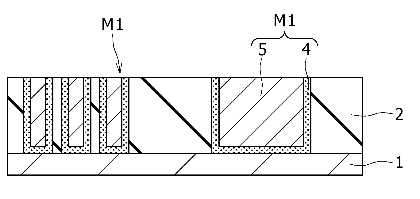
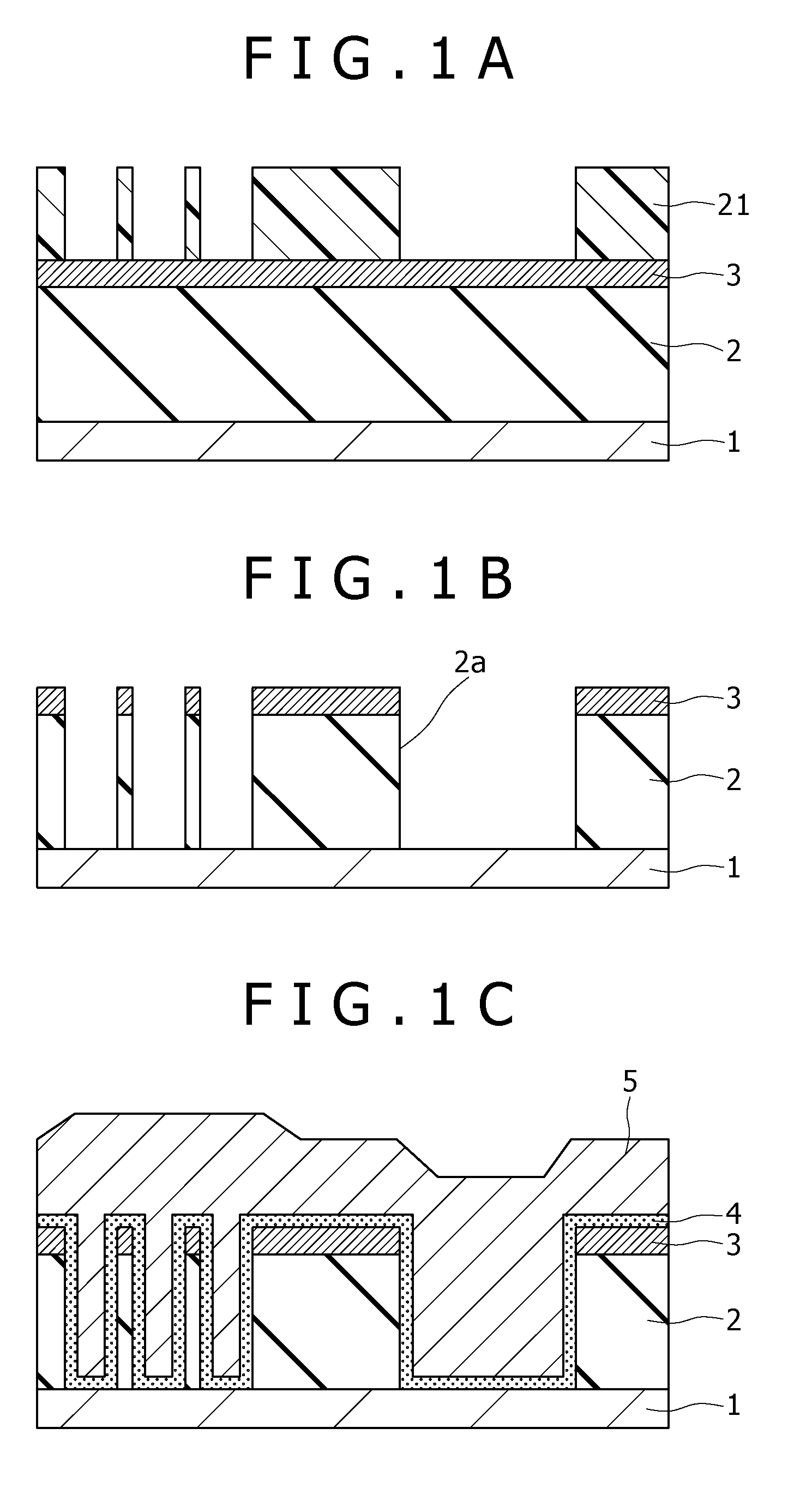
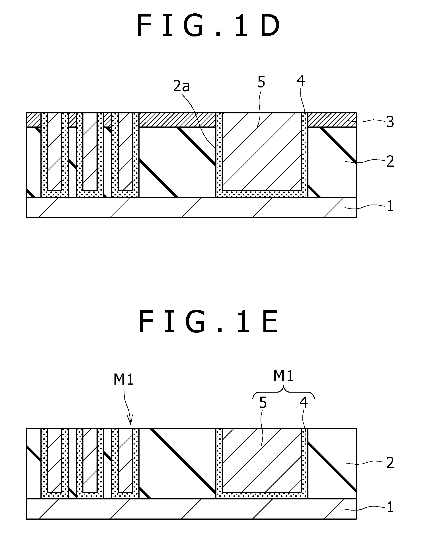
[0027] Embodiment 1 of the present invention will now be described in detail with reference to FIGS. 1A to 1E. In Embodiment 1 of the present invention, an example in which the present invention is applied to a single damascene process will be described below.

[0028] As shown in FIG. 1A, for example, a silicon carbide oxide film (SiOC) is deposited to be 150 nm thick on a base substrate 1 to form a first interlayer insulating film 2. The base substrate 1 is such that a transistor and other constituent elements are formed on a semiconductor substrate made of silicon or the like, and thus corresponds to a semiconductor substrate of the present invention. Subsequently, for example, a tantalum (Ta) film is deposited to be 10 nm thick for example on the first interlayer insulating film 2 to form a metal mask 3 made of a metal material. In this case, the silicon carbide oxide film is formed by using a parallel plate plasma enhanced CVD system for example. In formation of the silicon carbi...

embodiment 2

[0035] The example in which the present invention is applied to the single damascene process has been described so far in Embodiment 1, whereas an example in which the present invention is applied to a dual damascene process will be described below in detail in Embodiment 2. It should be noted that the lower level wiring will now be described by using the wiring structure which, for example, is manufactured through the processes of Embodiment 1.

[0036] As shown in FIG. 2A, after a predetermined after-treatment is performed, a silicon carbide (SiC) film is deposited on the first level wiring M1 to be 35 nm thick for example to form a diffusion preventing film 6 against Cu. The diffusion preventing film 6 thus formed functions as an oxidation preventing film as well for Cu. The silicon carbide film, for example, can be deposited by using the parallel plate plasma enhanced CVD system under the condition in which a pressure is set at 550 Pa and methylsilane (SiCH3) is used as the gas fo...

embodiment 3

[0048] The examples in which the present invention is applied to the single damascene structure and the dual damascene structure each having no barrier metal have been described so far in Embodiments 1 and 2, respectively. However, it is also possible to apply the present invention to the single damascene structure or the dual damascene structure each using a thin film barrier metal. An application example at this time will be described hereinafter. At that, since the processes in Embodiment 3 until the process shown in FIG. 2G are the same as those in Embodiment 2, their descriptions are omitted here for the sake of simplicity.

[0049] As shown in FIG. 3A, after the degassing treatment is performed, a tantalum (Ta) film, for example, is deposited to be 3 nm thick to form a barrier metal 12 for preventing Cu from diffusing into the second interlayer insulating film 7. In this case, for example, the tantalum (Ta) film is deposited by utilizing the directional sputtering method using t...


PUM


Abstract

Disclosed herein is a method of manufacturing a semiconductor device, including the steps of: forming an interlayer insulating film on a semiconductor substrate; forming a metal mask on the interlayer insulating film; forming a pattern trench in the metal mask and the interlayer insulating film by etching away parts of the metal mask and the interlayer insulating film; forming a conductive layer on the interlayer insulating film so as to fill in the pattern trench; and polishing the excessive conductive layer and the metal mask on the interlayer insulating film so as to leave the conductive layer in the pattern trench.

Description

CROSS REFERENCES TO RELATED APPLICATIONS [0001] The present invention contains subject matter related to Japanese Patent Application JP 2005-266865 filed in the Japanese Patent Office on Sep. 14, 2005, the entire contents of which being incorporated herein by reference. BACKGROUND OF THE INVENTION [0002] 1. Field of the Invention [0003] The present invention relates to a method of manufacturing a semiconductor device, and more particularly to a method of manufacturing a semiconductor device in which a single damascene process or a dual damascene process is adopted. [0004] 2. Description of the Related Art [0005] A copper (Cu) wiring gives a semiconductor device a lower resistance, a smaller capacity and higher reliability than an aluminum (Al) alloy wiring line gives. Thus, the importance of the copper wiring has increased in a micro-element in which circuit delay due to a parasitic resistance and a parasitic capacity of a wiring are dominant. In general, since unlike the Al alloy w...

Claims


Application Information

Patent Timeline
IPC IPC(8): H01L21/4763
CPCH01L21/76808H01L21/76829H01L21/76831H01L21/76873H01L21/76843H01L21/76864H01L21/7684
Inventor OOKA, YUTAKA
Owner TESSERA ADVANCED TECH
Why Eureka
Try Eureka