Electrostatic-capacitance-type acceleration sensor

a technology of acceleration sensor and capacitor, which is applied in the direction of speed/acceleration/shock measurement device testing/calibration, instruments, etc., can solve the problems of limited flexibility in wiring design, prone to further expansion of irregularities, and inability to multi-layer wiring, so as to achieve the effect of preventing electric characteristics

Active Publication Date: 2007-03-22
MITSUBISHI ELECTRIC CORP
View PDF11 Cites 22 Cited by
  • Summary
  • Abstract
  • Description
  • Claims
  • Application Information

AI Technical Summary

Benefits of technology

[0013] As configured above, in the electrostatic-capacitance-type acceleration sensor according to the present invention, the movable electrode of the acceleration detector can be prevente

Problems solved by technology

Moreover, because a single-crystalline silicon layer provided as the bonding frame is also used, flexibility in wiring design is limited, for example, the wiring cannot be multi-layered.
However, in a case of the polycrystalline silicon, surface irregularities generally become larger than that of single-crystalline silicon, and in addition, in a case of the stacked structure, the irregularities of the under layer of the bonding frame affect the polycrystalline-silicon surface in the upper layer; consequently, the irregularities have tended to become further larger.
When irregularities such as above become larger exceeding a certain level, sealing between the glas

Method used


Image

  • Electrostatic-capacitance-type acceleration sensor
  • Electrostatic-capacitance-type acceleration sensor
  • Electrostatic-capacitance-type acceleration sensor

Examples


embodiment 1

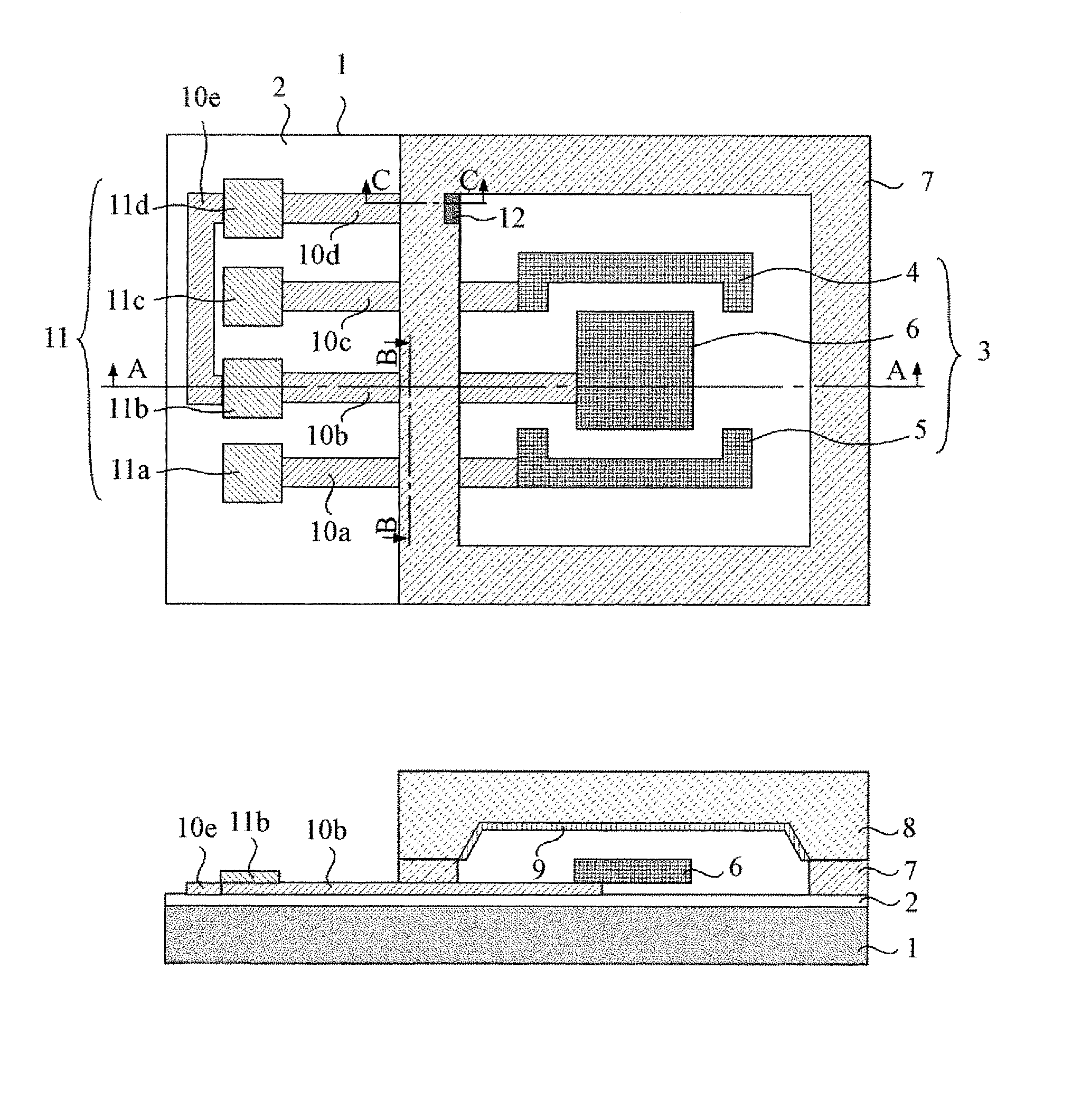
[0022] Hereinafter, Embodiment 1 according to the present invention is explained based on figures. FIG. 1 is a plane view illustrating an acceleration sensor in Embodiment 1 according to the present invention, and a cross-sectional view along A-A of the plane view. Acap is conveniently omitted in the plane view.

[0023] In FIG. 1, a semiconductor substrate 1 made of silicon has two main opposing faces parallel to each other, in which the thickness of the substrate is 400 μm and the size thereof 2.25 mm×2.5 mm in rectangular shape. A heat oxide film 2 whose thickness is 1.6 μm is provided, for insulation, on the upper face of the semiconductor substrate 1. An acceleration detector 3 whose thickness is 8 μm is provided over the semiconductor substrate 1 sandwiching the heat oxide film 2. The acceleration detector 3 is composed of a first fixed electrode 4, a second fixed electrode 5, and a movable electrode 6; thereby, acceleration is detected from variation of the capacitance between ...

embodiment 2

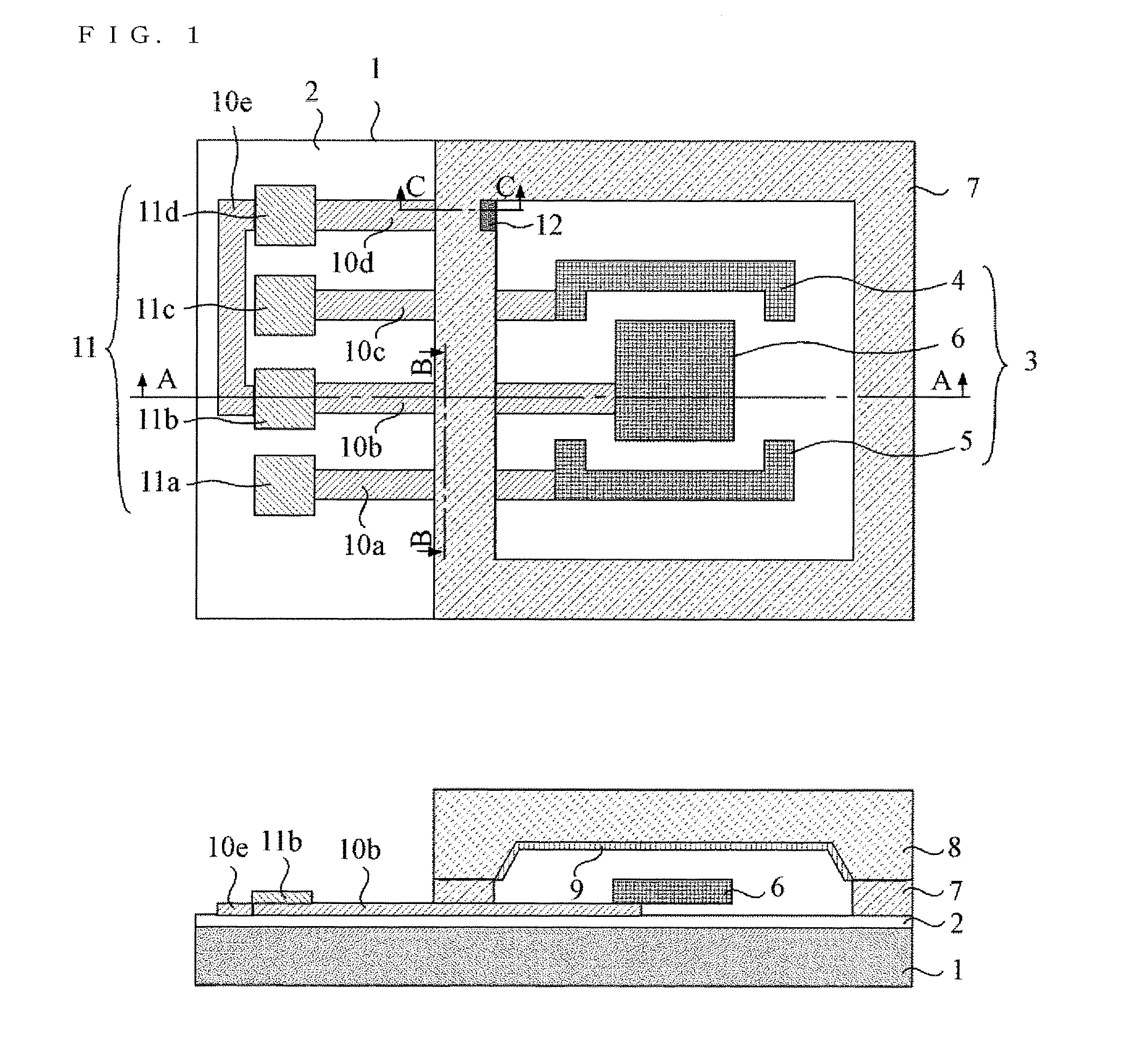
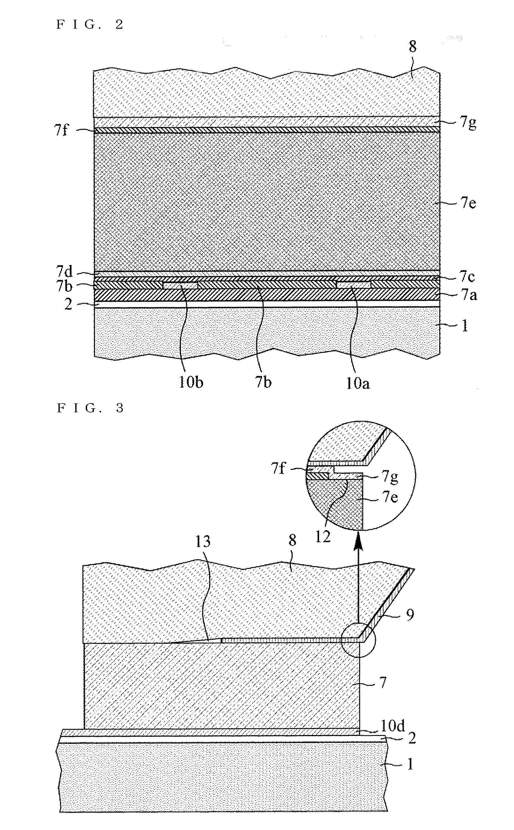
[0031] In above Embodiment 1, because the shielding film 9 is sandwiched by the bonding frame 7 and the cap 8, due to the thickness of the shielding film 9 itself, as represented in FIG. 3, a region 13 exists in which the bonding frame 7 and the cap 8 are not bonded together. According to the experimental result by the inventors, the region 13 that is not bonded has been found to horizontally extend in a distance of 100-500 times as long as the thickness of the shielding film 9. For example, in above Embodiment 1, the distance reaches 10-50 μm. The thicker the shielding film 9 becomes, the wider becomes the region in which the bonding cannot be performed, which causes the width of the bonded region to correspondingly decrease; however, because the width that must be bonded is predetermined by the product strength, it is more preferable that the thickness of the shielding film 9 is thinner. On the other hand, in a case in which the shielding film 9 is made of metal such as aluminum o...

embodiment 3

[0033] Embodiment 3 is another embodiment also coping with the above conflicting matters, in which a detailed structure is illustrated in FIG. 5, and a cross-sectional view along C-C of FIG. 5 is illustrated in FIG. 6. In FIG. 5, the thickness of the shielding film 9 is 0.8 μm, and the other elements are the same as those in FIG. 1 illustrating the structure in Embodiment 1. FIG. 6 represents a bonding structure of the bonding frame 7 with the cap 8, in which part of the shielding film 9 is sandwiched between the bonding frame 7 and the cap 8. On the portion, in which the shielding film 9 is sandwiched, of the bonding frame 7, a nick 71 having a depth that is equivalent to or a little smaller than the thickness of the shielding film 9 is formed entirely along the edge the bonding frame 7. By structuring the bonding frame 7 as described above, it becomes possible to provide the shielding film 9 without restriction from the film thickness; therefore, not only sufficient bonding streng...


PUM


Abstract

In an electrostatic-capacitance-type acceleration sensor, water, etc. penetrating into a sealed space incorporating an acceleration detector having a movable electrode 6, and sticking of the movable electrode 6 to a cap 8 due to static charge accumulated on the cap 8 during the anodic bonding being performed are prevented. A conductive shielding film 9 that can be extendedly transformed on the entire inner face of the cap 8 constituting the sealed space is provided, which is not only extendedly arranged so as to be sandwiched between a bonding frame 7 and the cap 8, but also electrically connected to the movable electrode 6; thereby, even if unevenness exists on the surface of the bonding frame 7, not only sufficient anodic bonding between the bonding frame 7 and the cap 8 becomes possible, but also the electric field due to the static charge accumulated in the cap 8 can be shielded.

Description

BACKGROUND OF THE INVENTION [0001] 1. Field of the Invention [0002] The present invention relates to electrostatic-capacitance-type acceleration sensors formed using semiconductor micro-machining technology. [0003] 2. Description of the Related Art [0004] In such acceleration sensors, in order to suitably vibrate their movable electrodes, which are mass bodies constituting acceleration detectors, in a vacuum or inert gas, the acceleration detectors need to be sealed with a separator such as a glass cap; meanwhile, in order to output a signal, from the acceleration detectors installed inside the glass cap, to the exterior, wires also need to be provided passing through the separator. [0005] Accordingly, an acceleration sensor is disclosed in Patent Document 1, in which a glass cap (cap) is anodically bonded to a bonding frame (frame) made of single-crystalline silicon in which impurities such as phosphorus are doped at a relatively low level, so as to form a tight-sealed space. That ...

Claims


Application Information

Patent Timeline
IPC IPC(8): G01P15/125
CPCB81B3/0008B81B7/0077G01P15/125G01P1/023B81B2201/0235G01P2015/0828G01P3/483
Inventor YAMAGUCHI, YASUOHORIKAWA, MAKIOOKUMURA, MIKASATOU, KIMITOSHI
Owner MITSUBISHI ELECTRIC CORP
Why Eureka
Try Eureka