
Light-emitting device comprising semiconductor nanocrystal layer free of voids and method for producing the same

Inactive Publication Date: 2007-03-29
SAMSUNG ELECTRONICS CO LTD
View PDF10 Cites 60 Cited by
  • Summary
  • Abstract
  • Description
  • Claims
  • Application Information

AI Technical Summary

Benefits of technology

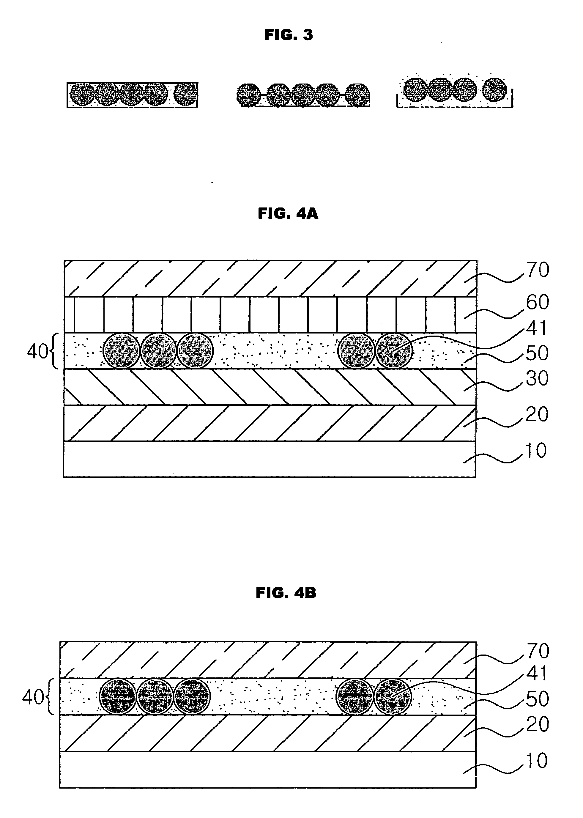
[0020] Accordingly, exemplary embodiments of the present invention provide a light emitting device having a semiconductor nanocrystal layer exhibiting high efficiency and excellent electrical stability by filling voids of the semiconductor nanocrystal layer with a filling.
[0021] In exemplary embodiments of the present invention, a light-emitting device includes a semiconductor nanocrystal layer whose voids are filled with a filling material so as to prevent occurrence of a current leakage through the voids and reduce the amount of an operating current, thereby enabling the device to have extended service life and high efficiency.
[0022] In other exemplary embodiments of the present invention, a light-emitting device includes a semiconductor nanocrystal layer whose voids are filled with a filling material so as to simplify the interfaces between the nanocrystal layer and its adjacent layers due to packaging effects arising from the filling, thereby enabling the device to have enhanced stability.

Problems solved by technology

When empty spaces are present between the nanocrystal particles of a nanocrystal layer used as a light-emitting layer in an electroluminescence device, holes do not combine with electrons at the nanocrystal particles to form excitons, and as a result, light emission is not achieved and current leakage occurs.
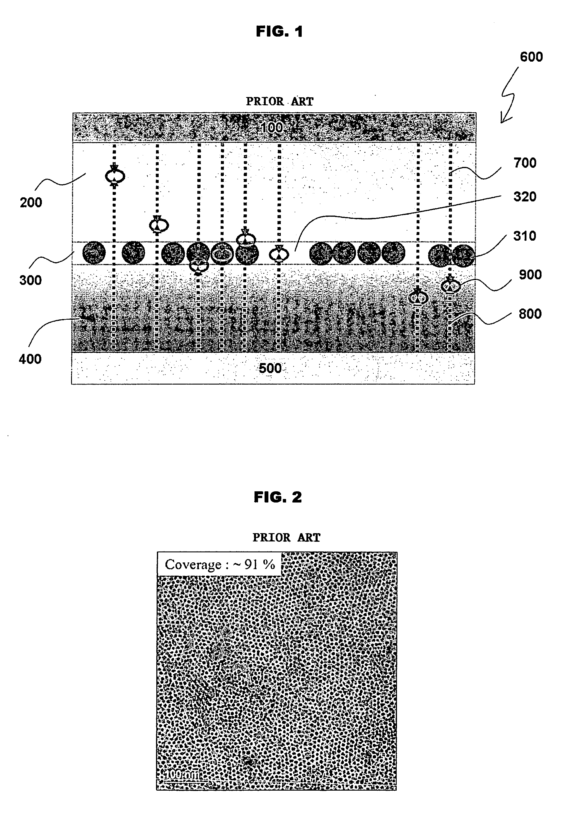
However, when the electrons meet the holes at voids 320 of the semiconductor nanocrystal layer 300, the electrons are directly bonded to the holes and current leakage is caused, leading to a reduction in the luminescence efficiency of the light-emitting device.
In addition, since the resistance at the voids 320 is extremely low, a large amount of current is concentrated on the voids 320 by Ohm's law, thus shortening the service life of the device and causing poor electrical stability of the device.
However, conventional processes have not been successful in the production of nanocrystal thin films free of empty spaces in view of their inherent characteristics.
This low transfer ratio causes occurrence of a large number of defects on nanocrystal thin films and makes it impossible to produce uniform monolayers.
This process, however, has a problem that the coverage is limited to a maximum of 70% despite the repeated dipping.
Since this process, in practice, causes the formation of nanoparticle aggregates, which leads to the occurrence of defects, it is disadvantageous in terms of degree of completeness.
However, these processes are not suitable for the production of uniform monolayers in which nanocrystals are uniformly applied.
When the nanocrystal thin film having voids is used to produce an electroluminescence device, a large amount of current is concentrated on the voids, thus shortening the service life of the device and damaging the electrical stability of the device.
Accordingly, in the case where the polymer thin film is used as a light-emitting layer of an electroluminescence device, the luminescence efficiency of the device is considerably low, making the polymer thin film unsuitable for the production of light-emitting devices.
However, no mention is made in the publication regarding the presence of voids between the quantum dots and current leakage arising from the voids.
As described above, the prior art light-emitting devices containing nanocrystals have focused on increasing the coverage of the nanocrystals, however a light-emitting device having a semiconductor nanocrystal layer exhibiting high efficiency and excellent electrical stability has not been obtained.

Method used


Image

  • Light-emitting device comprising semiconductor nanocrystal layer free of voids and method for producing the same
  • Light-emitting device comprising semiconductor nanocrystal layer free of voids and method for producing the same
  • Light-emitting device comprising semiconductor nanocrystal layer free of voids and method for producing the same

Examples


example 1

Fabrication of Light-Emitting Device Including Nanocrystal Layer Whose Voids are Filled with Filling Material

[0082] A TiO2 precursor (DuPont Tyzor, BTP, 2.5 wt % in butanol) was spin-coated on a patterned ITO substrate at 2,000 rpm under a nitrogen atmosphere for 30 seconds, dried under a nitrogen atmosphere for about 5 minutes, and annealed at 150° C. for 15 minutes to form an amorphous TiO2 thin film having a thickness of about 20 nm.

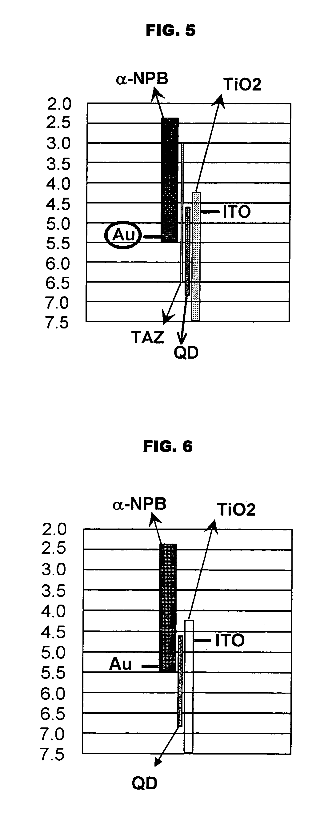
[0083] A solution (0.3 wt %) of red-emitting (642 nm) CdSe / ZnS core / shell structured quantum dots QD (diameter: about 6 nm, Evident Tech. Inc.) in chloroform was spin-coated on the TiO2 thin film at 2,000 rpm for 30 seconds, and dried at 50° C. for 5 minutes to arrange the quantum dots QD in a single layer. 3-(4-biphenyl)-4-phenyl-5-tert-butylphenyl-1,2,4-triazole (TAZ) was filled on the quantum dots QD to form a semiconductor nanocrystal layer. N,N′-di(naphthalen-1-yl)-N—N′-diphenyl-benzidine (a-NPB) was filled to a thickness of about 40 nm on the ...

experimental example 1

Comparison of Stability of Light-Emitting Devices

[0085] To evaluate the stability of the light-emitting devices produced in Example 1 and Comparative Example 1, the luminescence spectra, luminescence intensity per unit area, and changes in the amount of current flowing through the devices were measured at ambient temperature and pressure with increasing voltage applied to the devices.

[0086]FIGS. 7A and 7B are graphs showing luminescence spectra of the light-emitting devices produced in Example 1 and Comparative Example 1, respectively, with increasing voltage applied to the devices.

[0087]FIGS. 8A and 8B are graphs showing changes in luminescence intensity per unit area of the light-emitting devices produced in Example 1 and Comparative Example 1, respectively, with increasing voltage applied to the devices.

[0088] These graphs show that the intensity of light emitted from the light-emitting devices increases with increasing voltage applied to the devices.

[0089]FIGS. 9A and 9B ar...

experimental example 2

Comparison of Luminescence Efficiency of Light-Emitting Devices

[0091] To measure the luminescence efficiency of the light-emitting devices produced in Example 1 and Comparative Example 1, the luminescence intensity per unit current of the devices was measured at ambient temperature and pressure with increasing voltage applied to the devices.

[0092]FIGS. 10A and 10B are graphs showing changes in luminescence efficiency per unit current of the light-emitting devices produced in Example 1 and Comparative Example 1, respectively, with increasing voltage applied to the devices.

[0093] The graph of FIG. 10B shows that the luminescence efficiency per unit current of the light-emitting device produced in Comparative Example 1 gradually increases until it reaches a maximum at 13V and thereafter begins to rapidly decrease. In contrast, the graph of FIG. 10A shows that the luminescence efficiency of the light-emitting device produced in Example 1 is maintained at a high level from the beginni...


PUM


Abstract

A light-emitting device including a semiconductor nanocrystal layer and a method for producing the light-emitting device are provided. The light-emitting device includes a semiconductor nanocrystal layer whose voids are filled with a filling material. According to the light-emitting device, since voids formed between nanocrystal particles of the semiconductor nanocrystal layer are filled with a filling material, the occurrence of a current leakage through the voids is minimized, which enables the device to have extended service life, high luminescence efficiency, and improved stability.

Description

[0001] This application claims priority to Korean Patent Application No. 2005-90082, filed on Sep. 27, 2005 and all the benefits accruing therefrom under 35 U.S.C. § 119, and the contents of which in its entirety are herein incorporated by reference. BACKGROUND OF THE INVENTION [0002] 1. Field of the Invention [0003] The present invention relates to a light-emitting device having a semiconductor nanocrystal layer and a method for producing the light-emitting device. More particularly, the present invention relates to a light-emitting device having a semiconductor nanocrystal layer whose voids are filled with a filling material, and a method for producing the light-emitting device. [0004] 2. Description of the Related Art [0005] The control over the size of semiconductor nanocrystals exhibiting quantum confinement effects and enables control of electrical and optical properties of the nanocrystals. Based on this characteristic, semiconductor nanocrystals are applied to a variety of d...

Claims


Application Information

Patent Timeline
IPC IPC(8): H01L51/00
CPCB82Y20/00B82Y30/00H01L51/5012H01L33/18H01L33/08H10K50/11
Inventor CHOI, BYOUNG LYONGKIM, BYUNG KICHO, KYUNG SANGKWON, SOON JAECHOI, JAE YOUNG
Owner SAMSUNG ELECTRONICS CO LTD
Learn More