Insulated gate field effect transistor and manufacturing method thereof

a technology of field effect transistor and insulating gate, which is applied in the direction of basic electric elements, electrical equipment, semiconductor devices, etc., can solve the problem of limit on the improvement of high-frequency switching characteristics

Inactive Publication Date: 2007-03-29
SANYO ELECTRIC CO LTD
View PDF8 Cites 17 Cited by
  • Summary
  • Abstract
  • Description
  • Claims
  • Application Information

AI Technical Summary

Benefits of technology

[0018] The present invention provides an insulated gate field effect transistor that includes a semiconductor substrate of a first general conductivity type, a semiconductor layer of the first general conductivity type disposed on the semiconductor substrate so as to provide a drain region, a first channel region, a second channel region, a third channel region and a fourth channel region that are of a second general conductivity type and formed in the semiconductor layer, a first gate electrode disposed on the first and second channel regions and having a separation separating a first part of the first gate electrode from a second part of the first gate electrode, a second gate electrode disposed on the third and fourth channel regions and having a separation separating a first part of the second gate electrode from a second part of the second gate electrode, a body region of the second general conductivity type formed in the semiconductor layer and connecting the second and third channel regions, and a source region of the first general conductivity type formed in each of the channel regions.
[0019] The present invention also provides a method of manufacturing an insulated gate field effect transistor. The method includes providing a device intermediate comprising a semiconductor substrate of a first general conductivity type, a semiconductor layer of the first general conductivity type disposed on the semiconductor substrate and an insulating film disposed on the semiconductor layer, forming a first gate electrode on the insulating film having a separation so that the insulating film is exposed at a bottom of the separation of the first gate electrode, forming a second gate electrode on the insulating film having a separation so that the insulating film is exposed at a bottom of the separation of the second gate electrode, forming an impurity region of a second general conductivity type in the semiconductor layer between the first and second gate electrodes, forming a first source region of the first general conductivity type in the impurity region adjacent the first gate electrode, forming a second source region of the first general conductivity type in the impurity region adjacent the second gate electrode, and forming a body region of the second general conductivity ty

Problems solved by technology

Thus, there has been a limitation on improvement

Method used


Image

  • Insulated gate field effect transistor and manufacturing method thereof
  • Insulated gate field effect transistor and manufacturing method thereof
  • Insulated gate field effect transistor and manufacturing method thereof

Examples


first embodiment

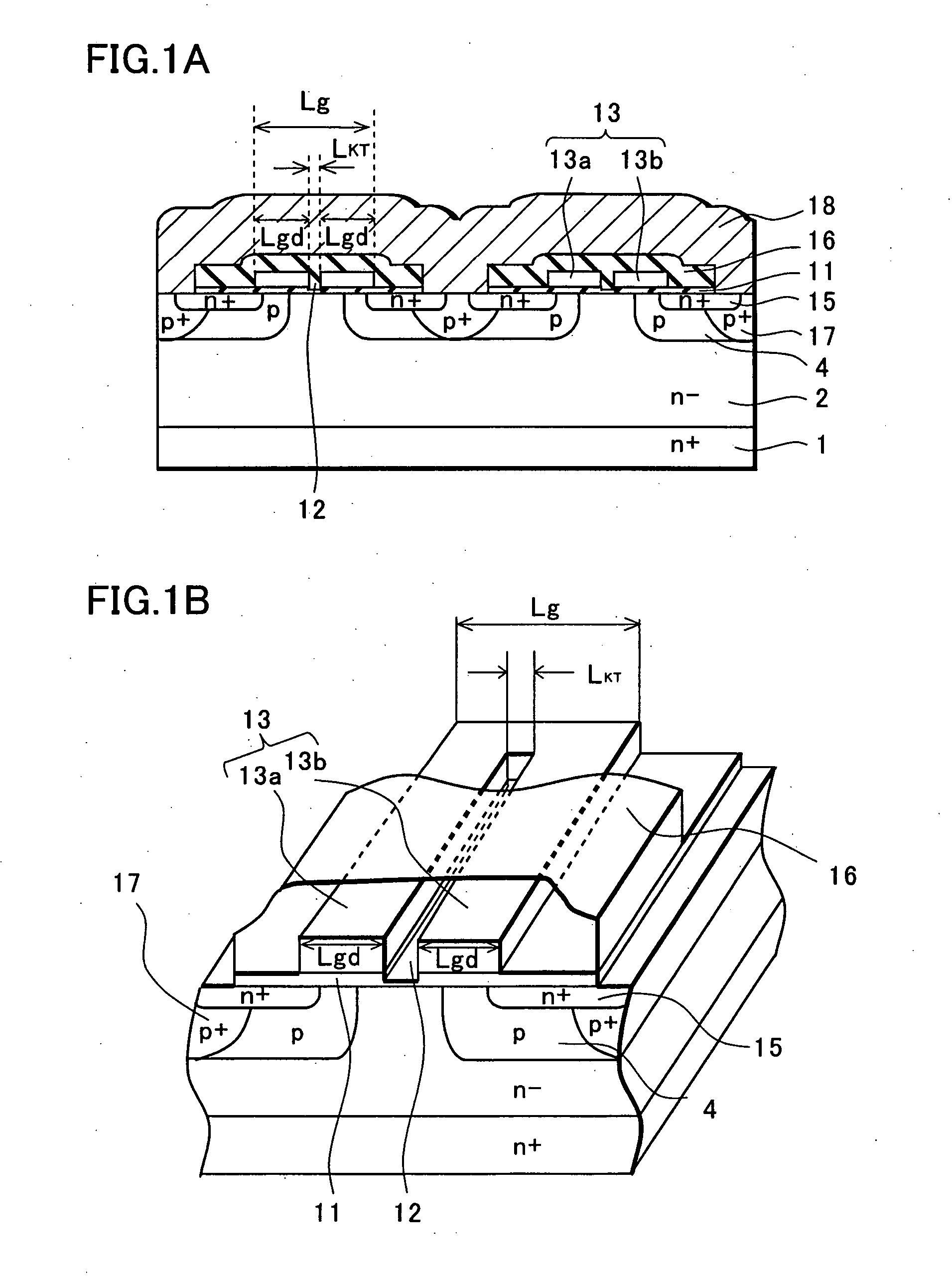
[0041]FIGS. 1A and 1B are views showing a structure of a MOSFET according to a FIG. 1A is a cross-sectional view and FIG. 1B is a perspective view.

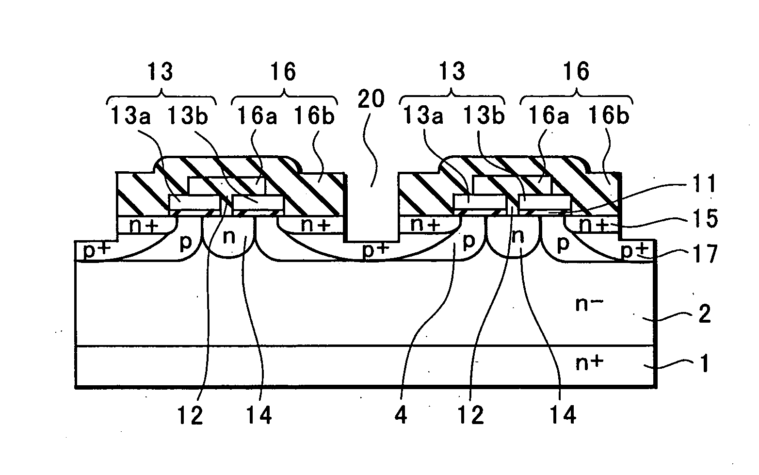
[0042] The MOSFET includes a semiconductor substrate 1, a semiconductor layer 2, a channel region 4, a gate electrode 13, a separation hole 12, a gate insulating film 11, an interlayer insulating film 16, a source region 15 and a body region 17.

[0043] A drain region is provided by superposing, for example, an n− type epitaxial layer 2 on an n+ type silicon semiconductor substrate 1, and by doing the like. In a surface of the n+ type epitaxial layer 2, p type channel regions 4 are provided. The plurality of channel regions 4 are provided in the surface of the epitaxial layer 2 by ion implantation and diffusion. Note that a low-resistance layer 1 may be formed by impurity diffusion in the semiconductor substrate 2.

[0044] A gate oxide film 11 is provided on the surface of the n− type epitaxial layer 2, and the gate electrode 13 (a gate le...

third embodiment

[0062] As shown in FIG. 4A, in the third embodiment, an n type impurity region 14 and channel regions 4 have approximately the same depth, and junction surfaces therebetween are vertically formed. In order to obtain such a structure, a separation width LKT of a separation hole 12, an impurity concentration of an n− type epitaxial layer 2, a gate length Lg of a gate electrode 13, and impurity concentrations of the n type impurity region 14 and the channel regions 4 are appropriately selected.

second embodiment

[0063] Moreover, as in the case of the second embodiment, ion implantation can be performed from the separation hole 12 which equally divides the gate electrode 13. Therefore, the n type impurity region 14 can be formed in a self-aligning manner below a center of the gate electrode 13. Moreover, the n type impurity region 14 can be formed accurately below the center of the gate electrode 13. Thus, it is possible to suppress a variation in extension of depletion layers.

[0064] Furthermore, since the n type impurity region 14 is formed by ion implantation from the separation hole 12, the impurity concentrations of the channel regions 4 and the n type impurity region 14 can be individually selected. Therefore, the n type impurity region 14 having a concentration higher than that of the n− type epitaxial layer 2 can be formed while maintaining the impurity concentration of the channel regions 4 at a desired value.

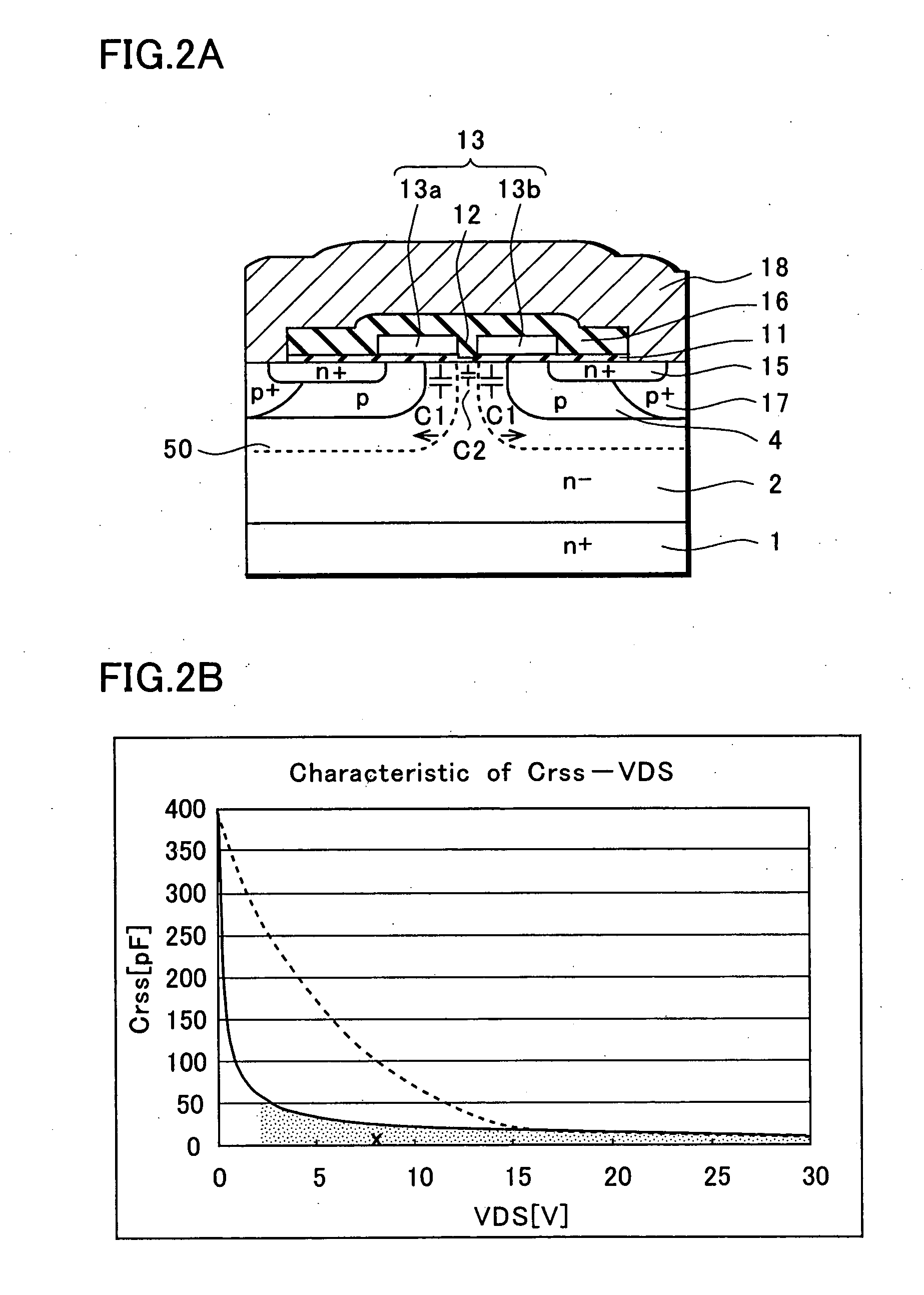
[0065]FIG. 4B is a characteristic graph showing a relationship between fee...


PUM


Abstract

A separation hole is provided in the center of the gate electrode. Accordingly, it is possible to suppress a drastic increase in feedback capacitance Crss in the case where drain-source voltage VDS is decreased and the width of the depletion layer is narrowed. Thus, high-frequency switching characteristics are improved. Moreover, n type impurities are implanted from the separation hole to form an n type impurity region between channel regions. Since a resistance in a portion below the gate electrode can be reduced, an on-resistance can be reduced. The n type impurity region can be formed in a self-aligning manner.

Description

BACKGROUND OF THE INVENTION [0001] Priority is claimed to Japanese Patent Application Number JP2005-284110 filed on Sep. 29, 2005, the disclosure of which is incorporated herein by reference in its entirety. [0002] 1. Field of the Invention [0003] The present invention relates to an insulated gate field effect transistor and a manufacturing method thereof. More particularly, the present invention relates to an insulated gate field effect transistor, which realizes reduction in feedback capacitance, and a manufacturing method thereof. [0004] 2. Description of the Related Art [0005] With reference to FIG. 16, an n-channel MOSFET will be described as an example of a conventional insulated gate field effect transistor. [0006] As shown in FIG. 16, a drain region 22 is provided by superposing an n− type semiconductor layer on an n+ type silicon semiconductor substrate 21. In a surface of the drain region 22, a plurality of p type channel regions 24 are provided. On a surface of the n− typ...

Claims


Application Information

Patent Timeline
IPC IPC(8): H01L21/337H01L21/8242H01L21/336
CPCH01L29/0878H01L29/41766H01L29/42372H01L29/7802H01L29/66712H01L29/66727H01L29/4238
Inventor KUSHIYAMA, KAZUNARIOKADA, TETSUYAOIKAWA, MAKOTOISHIDA, HIROYASUSAYAMA, YASUYUKI
Owner SANYO ELECTRIC CO LTD
Why Eureka
Try Eureka