Apparatus and methods for thermally processing undoped and lightly doped substrates without pre-heating

a technology of undoped and lightly doped substrates, applied in the direction of electrical apparatus, basic electric elements, semiconductor/solid-state device manufacturing, etc., can solve the problems of low resistance, low absorption of silicon wafers, and a deep change in the concentration of dopant atoms, so as to increase the absorption of an annealing radiation beam

a technology of undoped and lightly doped substrates, applied in the direction of electrical apparatus, basic electric elements, semiconductor/solid-state device manufacturing, etc., can solve the problems of low resistance, low absorption of silicon wafers, and a deep change in the concentration of dopant atoms, so as to increase the absorption of an annealing radiation beam

US20070072400A1Inactive Publication Date: 2007-03-29ULTRATECH INT INC

Image

  • Apparatus and methods for thermally processing undoped and lightly doped substrates without pre-heating
  • Apparatus and methods for thermally processing undoped and lightly doped substrates without pre-heating
  • Apparatus and methods for thermally processing undoped and lightly doped substrates without pre-heating

Examples


Embodiment Construction

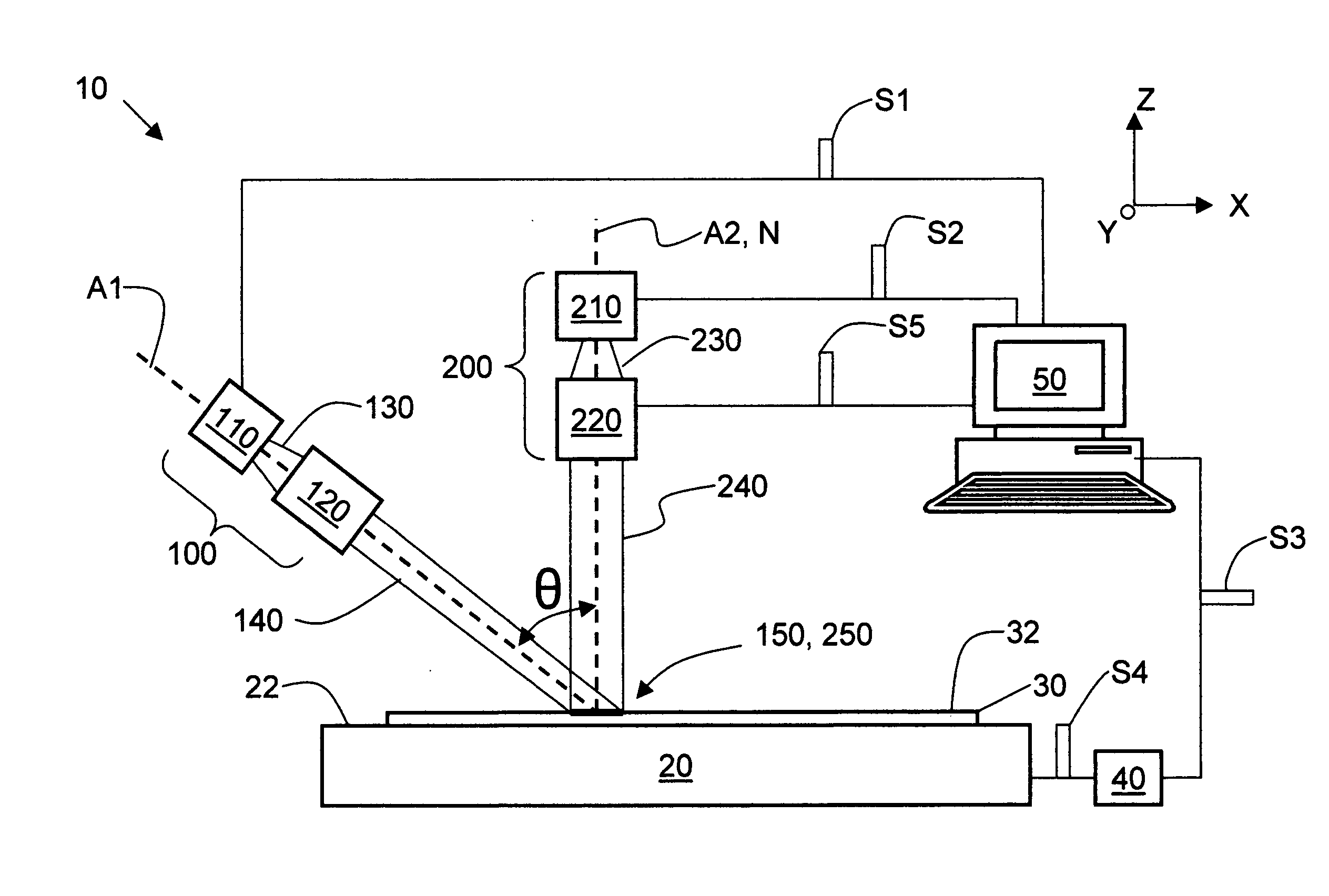
[0022] The present invention uses a relatively low-power, short-wavelength activation radiation beam concurrently with a relatively high-power, long-wavelength annealing radiation beam to process a semiconductor substrate. The short-wavelength activation beam has a photon energy greater than the semiconductor bandgap of the semiconductor substrate so that its absorption in the top surface of the substrate creates sufficient free carriers to absorb the longer-wavelength, annealing radiation beam. The annealing beam provides most of the energy required to generate a temperature high enough to process the substrate such as activating doped regions in the substrate. In the specific case of a 10.6 micron annealing beam operating on a silicon substrate, once the substrate surface reaches 400° C. or 500° C., the thermal generation of charge carriers is sufficient to absorb the long-wavelength radiation and short-wavelength activation is no longer required.

[0023] This approach obviates the...


PUM


Abstract

Apparatus for and methods of thermally processing undoped or lightly doped semiconductor wafers (30) that typically are not very absorptive of an annealing radiation beam (14) are disclosed. The apparatus (10) uses a relatively low power activating radiation beam (240) with a photon energy greater than the bandgap energy of the semiconductor substrate in order to generate free carriers (315) at and near the substrate surface (32). The free carriers so generated enhance the absorption by the substrate surface of the longer wavelength annealing radiation beam. The annealing radiation beam is thus able to rapidly heat the substrate surface and permit subsequent rapid cooling to obtain, for example, a high level of electrical activity (activation) of dopants (310) formed therein. The invention obviates the need to pre-heat the substrate in order to increase absorption of the annealing radiation beam when performing thermal processing.

Description

CROSS-REFERENCE TO RELATED APPLICATIONS [0001] The present invention is related to U.S. Pat. No. 6,747,245, entitled ā€œLaser Scanning Apparatus and Method for Thermal Processingā€, U.S. patent application Ser. No. 10 / 787,664 entitled ā€œLaser Scanning Apparatus and Methods for Thermal Processingā€ filed on Feb. 26, 2004, U.S. patent application Ser. No. 10 / 806,014, entitled ā€œLaser Scanning Apparatus and Methods for Thermal Processingā€ filed on Mar. 22, 2004 and published as U.S patent application Ser. No. 2004 / 0173585 on Sep. 09, 2004, U.S. patent application Ser. No. 10 / 674,106 entitled ā€œMethod of Annealing Undoped Silicon Substratesā€ filed on Sep. 29, 2003 and U.S. patent application Ser. No. 10 / 762,861 entitled ā€œLaser Thermal Annealing of Lightly Doped Silicon Substratesā€ filed on Jan. 22, 2004, all of which are assigned to the present Assignee Ultratech, Inc. of San Jose, Calif., and all of which are incorporated by reference herein.BACKGROUND OF THE INVENTION [0002] 1. Field of the ...

Claims


Application Information

Patent Timeline
29 Mar 2007
Publication
US20070072400A1
IPC
H01L21/20
CPC
H01L21/2026; H01L21/67115; H01L21/324; H01L21/268; H01L21/02683; H01L21/02678; H01L21/02532; H01L21/02381
Inventors
BAKEMAN, PAUL