Stencil masks, method of manufacturing stencil masks, and method of using stencil masks

a stencil mask and manufacturing method technology, applied in the field of stencil masks, can solve the problems of inability to accurately control the irradiation area, inability to use conventional stencil masks, uneven density of charged particles in the irradiation area, etc., and achieve the effect of convenient manufacturing, convenient manufacturing of stencil masks, and convenient use of semiconductor devices

Inactive Publication Date: 2007-04-05
TOYOTA JIDOSHA KK
View PDF14 Cites 10 Cited by
  • Summary
  • Abstract
  • Description
  • Claims
  • Application Information

AI Technical Summary

Benefits of technology

[0043] With this manufacturing method, the second layer of the stencil mask is formed using the semiconductor lower layer, and the first layer of the stencil mask is formed using the semiconductor upper layer. The stencil mask of the present invention can thus be manufactured easily.
[0044] When the stencil mask of the present invention is utilized, deformation of the stencil mask is suppressed when the charged particles are irradiated. Furthermore, when the

Problems solved by technology

However, when the charged particles were introduced with this type of the stencil mask, a part of the irradiation area was masked by the beam member, and the density of the charged particles becomes uneven within the irradiation area.
However, in this case, the scattering phenomenon causes the charged particles to be introduced over a wide area, and it is no longer possible to accurately control the irradiation area to the predetermined pattern at the surface of the semiconductor substrate.
In this case, the conventional stencil mask cannot be utilized.
Furthermore, when this type of stencil mask having beam members was utilized and the charged particles were introduced, the temperature of the stencil mask is increased because the charged particles collide with the stencil mask, and as a result, deformation of the stencil mask frequently occurred.
Deformation of the stencil mask causes the problems that the irradiation area of the

Method used


Image

  • Stencil masks, method of manufacturing stencil masks, and method of using stencil masks
  • Stencil masks, method of manufacturing stencil masks, and method of using stencil masks
  • Stencil masks, method of manufacturing stencil masks, and method of using stencil masks

Examples


first embodiment

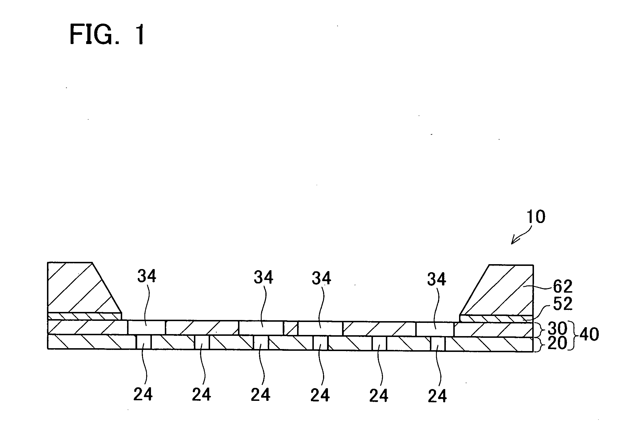
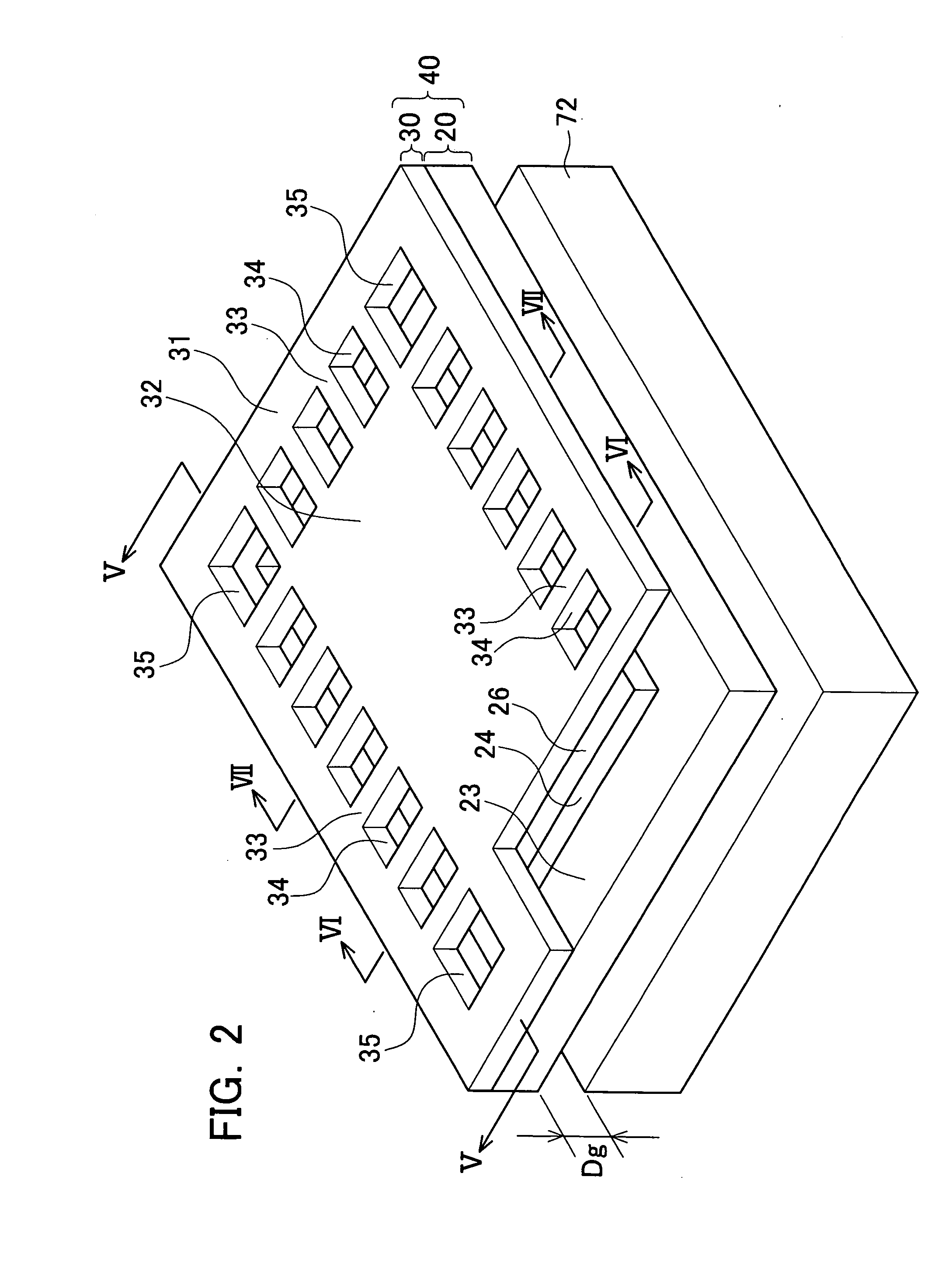
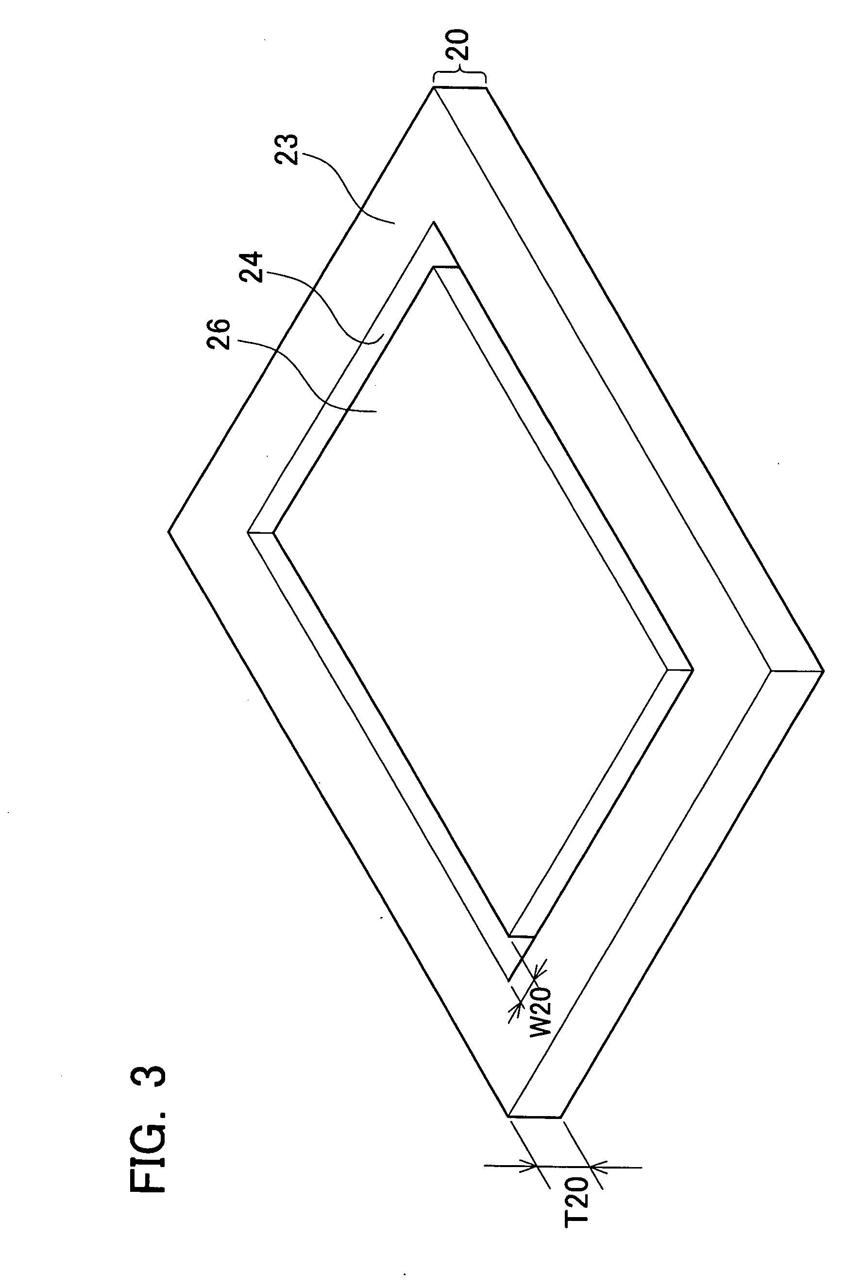
[0097] An embodiment of a stencil mask will be described below with reference to figures. A stencil mask of the present embodiment is used for limiting an irradiation area of ionized atoms to a predetermined shape on the surface of the semiconductor substrate and locally introducing ionized atoms into the semiconductor substrate. The area where the ionized atoms are introduced and the area where the ionized atoms are not introduced are controlled by the stencil mask. When the stencil mask of the present embodiment is utilized, it is possible to form the ion introducing area in a loop shape at the surface of the semiconductor substrate. Moreover, the ion introducing area is not restricted to being formed in a loop shape, but can be formed in various shapes by modifying the pattern of penetrating holes formed in the stencil mask.

[0098] A simple description of the figures will be given first. FIG. 1 is a longitudinal cross-sectional view schematically showing the basic configuration o...

second embodiment

[0171] In the second embodiment, the method of utilizing a stencil mask to manufacture a semiconductor device having a switching function will be described. The semiconductor device of the present embodiment is a level shift circuit (an example of a compound device) in which a high potential circuit region and a low potential circuit region are formed in one semiconductor substrate. FIG. 37 schematically shows a plan view of a level shift circuit 1000.

[0172] The level shift circuit 1000 comprises a high potential circuit region 1012, a low potential circuit region 1011, and a mediating circuit region 1010 that connects the two. A semiconductor switching element that performs switching of high voltage power is formed in the high potential circuit region 1012. A control circuit for switching the semiconductor switching element ON and OFF, and that operates at low potential is formed in the low potential circuit region 1011. The high potential circuit region 1012, the low potential ci...


PUM


Abstract

The present invention presents a stencil mask in which various surface patterns can be formed, and in which deformation is suppressed when charged particles are introduced. A stencil mask of the present invention is provided with a semiconductor stack. A first penetrating hole corresponding to an ion introducing area is formed in a first semiconductor layer of the semiconductor stack, and second penetrating holes are formed in a second semiconductor layer, these second penetrating holes having a width greater than the width of the first penetrating hole. The first penetrating hole and the second penetrating holes communicate and pass through the semiconductor stack. Beam members extending between adjacent second penetrating holes connect portions of the first semiconductor layer separated by the first penetrating hole.

Description

CROSS-REFERENCE TO RELATED APPLICATION [0001] The present application claims priority based on Japanese Patent Application No. 2005-225453, filed on Aug. 3, 2005, the contents of which are hereby incorporated by reference within this application. BACKGROUND OF THE INVENTION [0002] 1. Field of the Invention [0003] The present invention relates to a stencil mask for limiting an irradiation area of charged particles on a surface of a substrate to a predetermined shape. The charged particles may be ionized atoms, electrons, etc. The stencil mask is suitable for manufacturing a semiconductor device that works as a switching element, light emitting element, light detecting element. The stencil mask is also suitable for manufacturing a micromachine. [0004] 2. Description of the Related Art [0005] In the process of manufacturing the semiconductor device, a process is widely used wherein a local area on a surface of a semiconductor substrate is irradiated with the charged particles, and an a...

Claims


Application Information

Patent Timeline
IPC IPC(8): G03F1/00A61N5/00G21G5/00G03C5/00G03F1/20G03F1/68H01L21/266
CPCB82Y10/00B82Y40/00G03F1/20H01J37/3174H01J2237/31711
Inventor NISHIWAKI, TSUYOSHITOJIMA, HIDEKI
Owner TOYOTA JIDOSHA KK
Why Eureka
Try Eureka