Insulated gate bipolar transistor

a bipolar transistor and insulated gate technology, applied in the direction of transistors, electrical devices, semiconductor devices, etc., can solve the problems of undetectable increase of the operating forward voltage of the igbt, and achieve the effects of reducing the tail current, rapid annihilation, and improving the switching property

Inactive Publication Date: 2007-04-12
SANKEN ELECTRIC CO LTD
View PDF9 Cites 63 Cited by
  • Summary
  • Abstract
  • Description
  • Claims
  • Application Information

AI Technical Summary

Benefits of technology

[0012] When IGBT is turned from on to off, second recombination region (23) acquires minority carriers accumulated around second recombination region (23) in buffer region (11) to rapidly annihilate minority carriers, thereby to effectively reduce tail current for

Problems solved by technology

However, a prior art exposure technique has a process for uniformly irradiating radiation over a whole semiconducting substrate with the built-in IGBT and diode, and therefore, it disadvantageously forms crystal defects in N type b

Method used


Image

  • Insulated gate bipolar transistor
  • Insulated gate bipolar transistor
  • Insulated gate bipolar transistor

Examples


Embodiment Construction

[0022] Embodiments of the insulated gate bipolar transistor according to the present invention will be described hereinafter in connection with FIGS. 1 to 7 of the drawings.

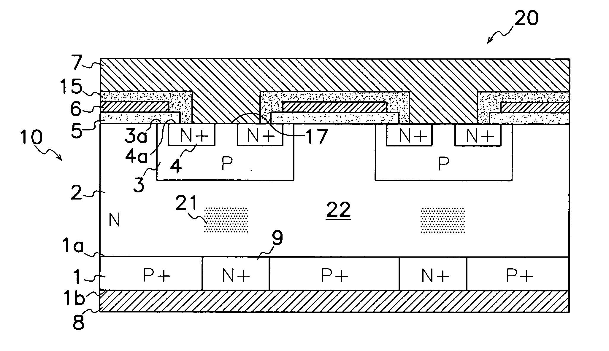
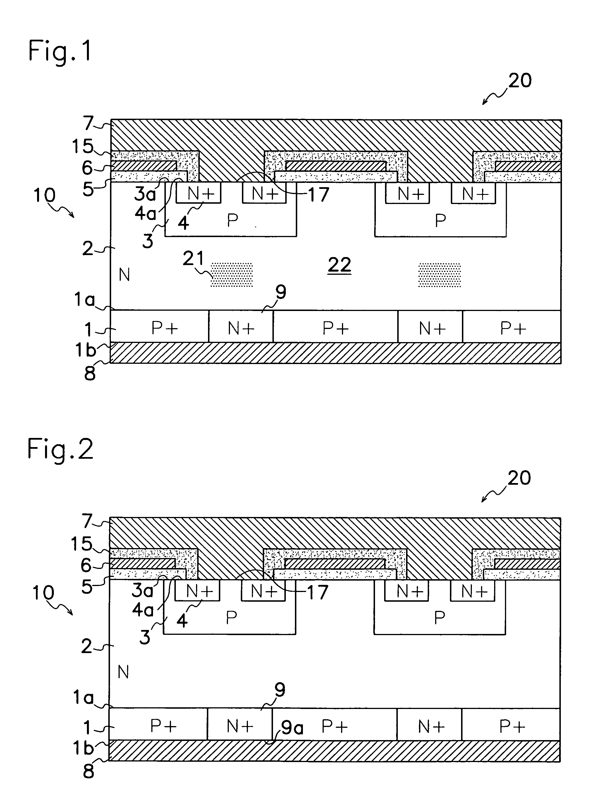
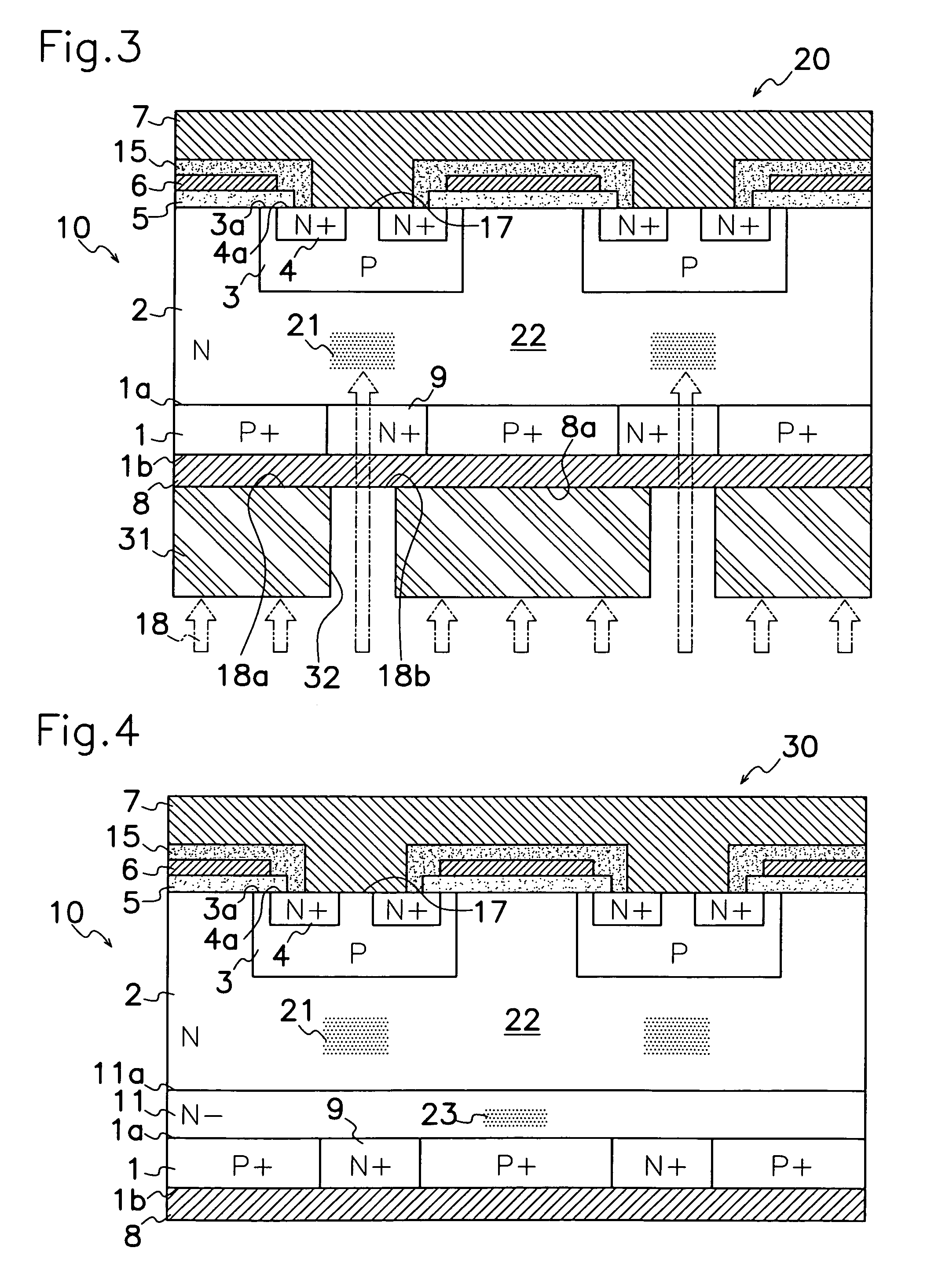
[0023] As shown in FIG. 1, IGBT 20 according to a first embodiment of the present invention comprises a semiconducting base plate or substrate 10 formed of for example silicon monocrystal which comprises a P+ type collector region 1, an N type or first base region 2 formed on one or upper surface of P+ collector region 1, P type or second base regions 3 formed adjacent to N type base region 2, and N+ type emitter regions 4 formed adjacent to P type base region 3. IGBT 20 further comprises gate electrodes 6 formed in spaced relation to P type base regions 3 via gate insulating film or insulator 5, an emitter electrode 7 formed on each upper or one main surface 3a, 4a of P type base region 3 and N+ type emitter region 4 in spaced relation to gate electrodes 6 through an insulating interlayer film 15, and a collect...


PUM


Abstract

An IGBT is provided which comprises N+ type extended region 9 sectively formed in P+ type collector region 1 to define a built-in diode in cooperation with N+ type extended region 9, an N− type base region 2 and a P− type base region 3 in semiconducting substrate 10. N− type base region 2 comprises a recombination region 21 developed between P type base region 3 and collector electrode 8 to acquire minority carriers accumulated around recombination region 21 in first base region 2 by recombination region 21 for improvement in recovery property of the diode without increasing voltage in the forward direction since recombination region 21 does not reach between and beneath adjoining second base regions 3 in N type base region 2 for current path.

Description

TECHNICAL FIELD [0001] This invention relates to an insulated gate bipolar transistor, in particular, of the type having a built-in diode. BACKGROUND OF THE INVENTION [0002] A typical insulated gate bipolar transistor (IGBT) comprises: a semiconducting substrate which comprises a P+ type collector region, an N type base region formed on P+ type collector region, a P type base region formed on N type base region, and N+ type emitter regions formed on an upper surface of P type base region; gate electrodes each formed in spaced relation to P type base region through an insulator; an emitter electrode formed in spaced relation to gate electrode through an insulating interlayer film and on each upper surface of P type base region and N+ type emitter region; and a collector electrode formed on a bottom surface of P+ type collector region. A part of P type base region sandwiched between N+ type emitter region and N type base region is opposite to gate electrode through gate insulation fil...

Claims


Application Information

Patent Timeline
IPC IPC(8): H01L29/76
CPCH01L29/0834H01L29/32H01L29/36H01L29/66333H01L29/7395H01L29/70
Inventor KONO, YOSHINOBU
Owner SANKEN ELECTRIC CO LTD
Why Eureka
Try Eureka