Method for manufacturing a compound semiconductor device having an improved via hole

a semiconductor device and via hole technology, applied in the direction of semiconductor devices, basic electric elements, electrical equipment, etc., can solve the problems of reducing the thickness of the wafer, forming a tapered via hole, and reducing the etching rate, so as to achieve no softening point, increase the etching rate, and high softening point

Inactive Publication Date: 2007-04-12
MITSUBISHI ELECTRIC CORP
View PDF8 Cites 53 Cited by
  • Summary
  • Abstract
  • Description
  • Claims
  • Application Information

AI Technical Summary

Benefits of technology

[0006] According to the present invention, the wafer is bonded to the support substrate with an adhesive having a softening point higher than 200° C. Since the adhesive has such a high softening point, one can assume that it has substantially no softening point, allowing for etching at high temperature. Therefore, it is possible to increase the etching rate and improve the perpendicularity of the sidewalls of the via hole. Further, the improvement in the shape of the via hole will lead to enhanced heat dissipation characteristics of the wafer. Furthermore, the above arrangement reduces the cost for the grinding required to reduce the thickness of the wafer, as well as facilitating handling of the wafer.

Problems solved by technology

This results in a reduced etching rate and formation of a via hole having a tapered shape if its depth is large.
However, a reduction in the thickness of the wafer increases the difficulty of handling the wafer.

Method used


Image

  • Method for manufacturing a compound semiconductor device having an improved via hole
  • Method for manufacturing a compound semiconductor device having an improved via hole

Examples


first embodiment

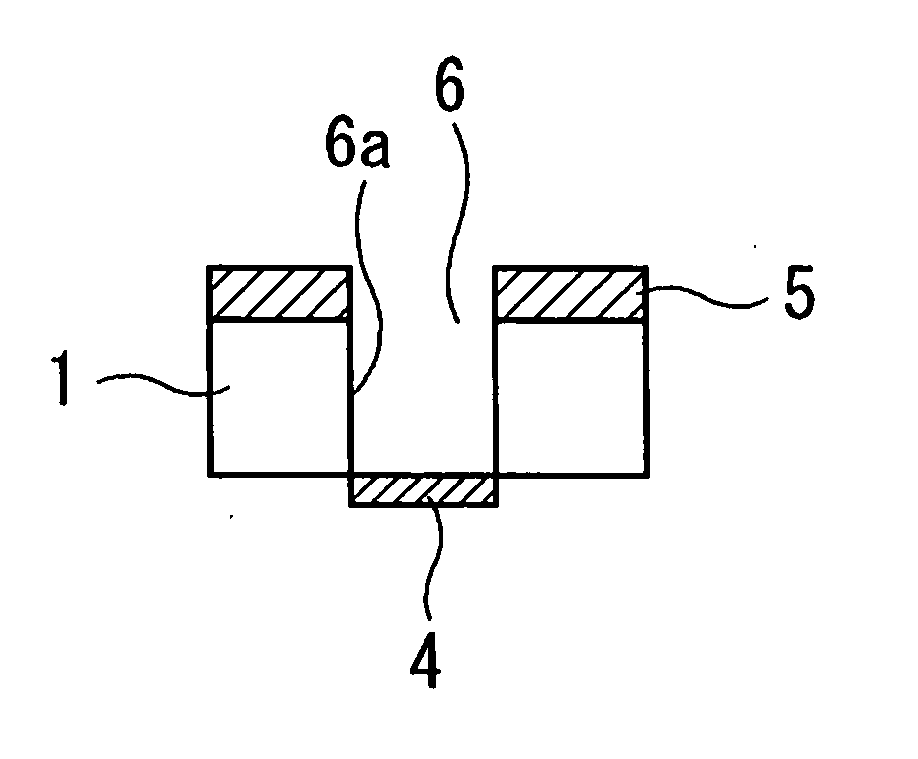
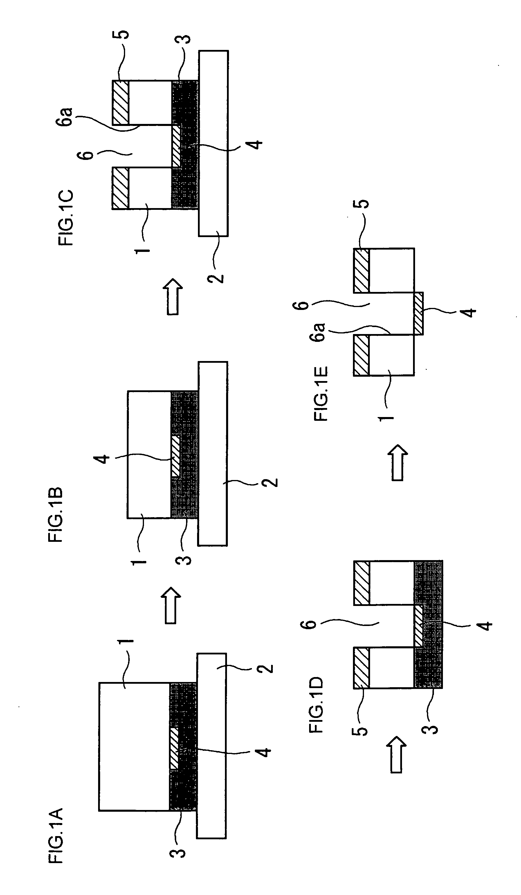
[0014]FIGS. 1A to 1E show cross-sectional views schematically illustrating a via hole forming process employed by a method for manufacturing a compound semiconductor device according to a first embodiment of the present invention. Specifically, FIGS. 1A to 1E show the sequential process steps of the via hole forming process. Referring to the figure, reference numeral 1 denotes a SiC wafer formed of single-crystal SiC, i.e., a substrate material for the compound semiconductor device; 2, a support substrate made up of a GaAs wafer and used to hold the SiC wafer 1; 3, an adhesive for bonding the SiC wafer 1 to the support substrate 2; 4, an electrode of gold (Au) deposited on a predetermined region of the principal surface of the SiC wafer 1 (or the undersurface of the SiC wafer 1 in the figures); 5, a Ni layer provided on predetermined regions on the rear side of the SiC wafer 1; 6, a via hole; and 6a, sidewalls of the via hole. It should be noted that according to the present embodim...


PUM


Abstract

In a method for manufacturing a compound semiconductor device, a principal surface of a SiC wafer, on which a compound semiconductor device is located, is bonded to a support substrate with an adhesive having a softening point higher than 200° C. A via hole is formed dry etching, including supplying a fluorine-containing etching gas to a rear side of the SiC wafer. Thereafter, the support substrate and the adhesive are removed. Preferably, the adhesive is formed by reacting one material coating the principal surface of the SiC wafer, and another material coating the support substrate.

Description

FIELD OF THE INVENTION [0001] The present invention relates to a method for manufacturing a compound semiconductor device, which can be suitably used to manufacture high frequency transistors, MMICs (Microwave Monolithic Integrated Circuits), etc. that employ compound semiconductors. More particularly, the invention relates to an improved method for forming a via hole, which greatly enhances the heat dissipation characteristics of the device. BACKGROUND ART [0002] A conventional method for manufacturing a compound semiconductor device includes the following sequential steps: forming a via hole by dry etching using a photosensitive polyimide mask; removing the photosensitive polyimide mask; depositing a metal wire extending from within the via hole to the vicinity of the MMIC device on the principal surface of the substrate; covering the principal surface of the substrate with a photosensitive polyimide resin so as to fill the via hole; bonding the principal surface side of the compo...

Claims


Application Information

Patent Timeline
Patent Type & Authority Applications(United States)
IPC IPC(8): H01L21/00H01L21/28H01L21/31H01L21/3205H01L21/469
CPCH01L21/6835H01L21/76898H01L2221/68345
Inventor SHIRAHAMA, TAKEOMIYAKUNI, SHINICHIKITANO, TOSHIAKIIINO, TAKAHIRONISHIZAWA, KOUICHIROU
Owner MITSUBISHI ELECTRIC CORP
Why Eureka
Try Eureka