Liquid-crystal display device with thin-film transistors and method of fabricating the same

a thin-film transistor and display device technology, applied in semiconductor devices, instruments, electrical devices, etc., can solve the problems of deterioration of display quality, likely to occur corrosion of transparent conductive materials, and likely to occur degradation of display quality, so as to reduce production costs and reduce the effect of quality

Active Publication Date: 2007-04-19
VISTA PEAK VENTURES LLC
View PDF1 Cites 4 Cited by
  • Summary
  • Abstract
  • Description
  • Claims
  • Application Information

AI Technical Summary

Benefits of technology

[0029] Accordingly, an object of the present invention is to provide a LCD device that solves the previously-described two problems of “corrosion of the transparent conductive layers” and “contact resistance increases” without arising the above-described first to third disadvantages (i.e. the step coverage degradation due to the thickness increase of the interconnection line itself, the step coverage degradation due to the formation of undercut portions, and productivity reduction and fabrication cost increase), and a method of fabricating the LCD device.

Problems solved by technology

Since the resistance increase of the said interconnection lines causes transmission delay of electric signals, the display quality degradation is likely to arise.
If the said lines are narrowed, however, their resistance will increase and thus, the display quality will degrade due to the transmission delay of signals.
Therefore, there is a problem that corrosion is likely to occur in the transparent conductive material due to electrochemical reaction caused by the developing or etching solution used for patterning the transparent conductive layer.
In this case, an aluminum oxide (Al2O3) layer with an insulating property is formed at the interface between the Al layer and the transparent conductive material, arising another problem that the contact resistance between them increases.
The first disadvantage is the step coverage degradation of an overlying layer or layers located on or over the interconnection lines.
The second disadvantage is the possibility that the step coverage of an overlying layer or layers located on or over the interconnection lines degrades conspicuously.
Due to the undercut portions, the step coverage of the overlying layer or layers may deteriorate.
The third disadvantage is the productivity reduction and fabrication cost increase.
This reduces the productivity and as a result, the fabrication cost increases.
Thus, a disadvantage that the fabrication cost of the LCD device increases by the cost for preparing the CVD apparatus or the sputtering apparatus and the target occurs.
In addition, there is another disadvantage that the formation process of the silicide layer accelerates or promotes the formation of hillocks and / or voids of the Al layer due to thermal history.
Therefore, there are the same disadvantages as those of the conventional interconnection structure shown in FIG. 1.

Method used


Image

  • Liquid-crystal display device with thin-film transistors and method of fabricating the same
  • Liquid-crystal display device with thin-film transistors and method of fabricating the same
  • Liquid-crystal display device with thin-film transistors and method of fabricating the same

Examples


first embodiment

Configuration of LCD Device

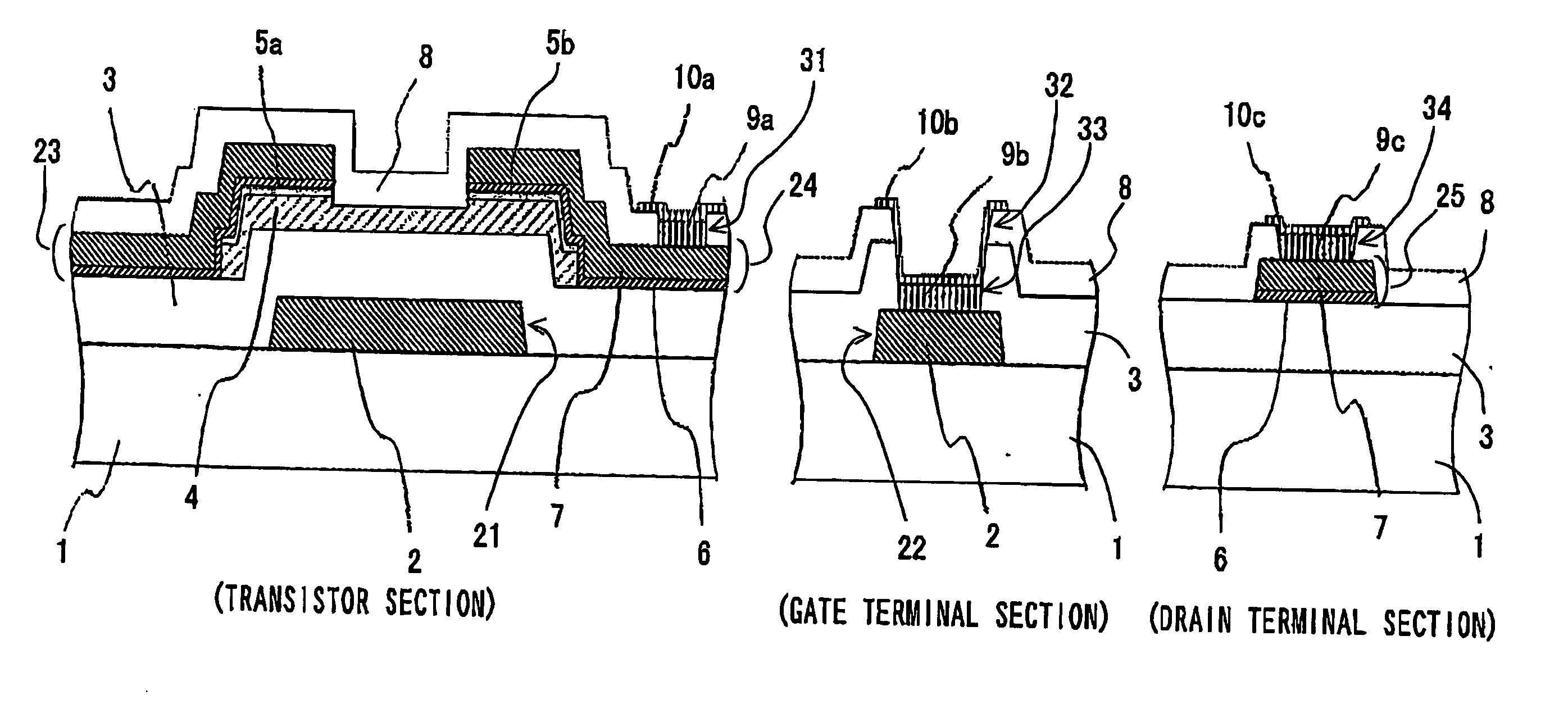
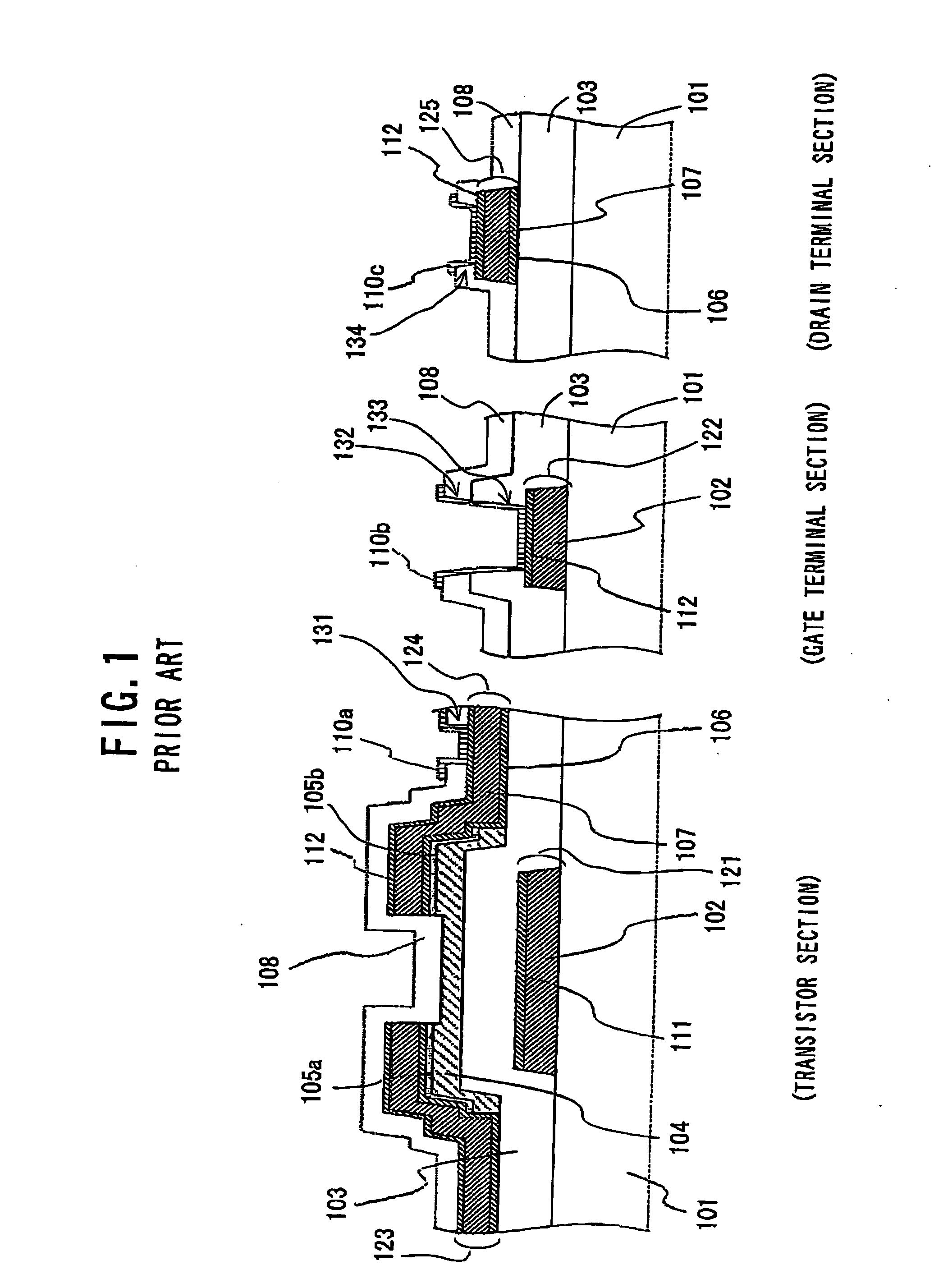
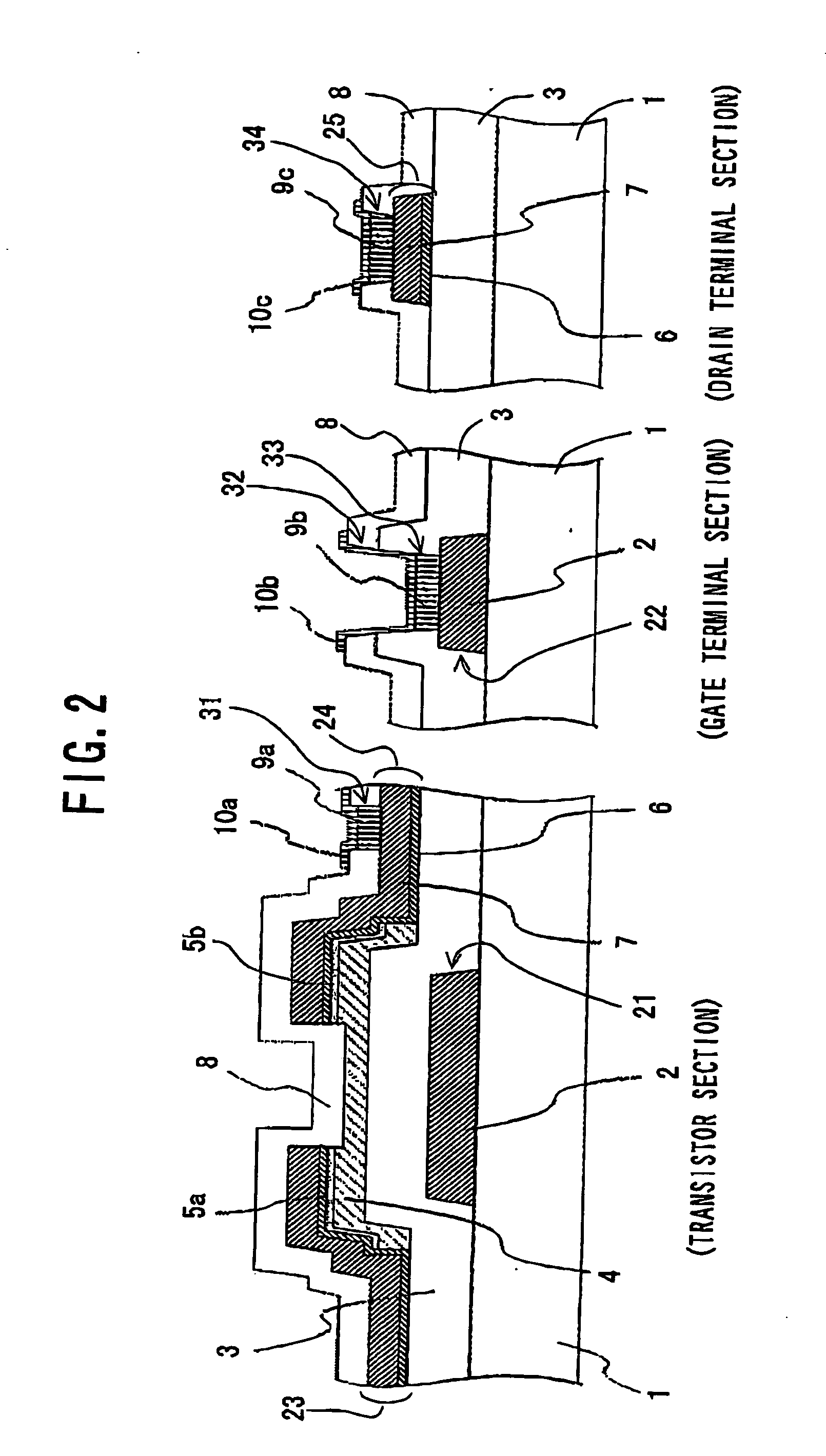
[0088]FIG. 2 schematically shows the configuration of a LCD device with TFTs according to a first embodiment of the present invention. In FIG. 2, the structures of the transistor section including one of the TFTs, the gate terminal section of the gate electrode line connected to the gate electrode of the TFT, and the drain terminal section of the drain electrode line connected to the drain electrode of the TFT are shown.

[0089] Here, each of the TFTs has the inverted staggered structure and the etched channel structure. However, the invention is applicable to any other type or structure of the TFT having wiring or interconnection lines comprising at least patterned Al or Al alloy layer.

[0090] As shown in FIG. 2, gate electrodes 21 and gate electrode lines 22 are formed on a rectangular glass plate 1. Each of the gate electrodes 21 is formed by a patterned Al alloy layer 2 to have a single-layer structure. Each of the gate electrode lines 22 is formed by...

second embodiment

[0122]FIG. 5 schematically shows the configuration of a LCD device with TFTs according to a second embodiment of the present invention. In FIG. 5, similar to FIG. 2, the structures of the transistor section including one of the TFTs, the gate terminal section of the gate electrode line connected to the gate electrode of the TFT, and the drain terminal section of the drain electrode line connected to the drain electrode of the TFT are shown.

[0123] The configuration of the LCD device according to the second embodiment is the same as the LCD device according to the above-described first embodiment of FIG. 2, except that gate electrodes 21a and gate electrode lines 22a have a two-layer structure comprising an Al layer and a conductive barrier layer (a lower barrier layer) made of tungsten (W) or the like stacked beneath the Al layer. Therefore, explanation about the same configuration is omitted here for simplification by respectively attaching the same reference numerals to the same e...


PUM

PropertyMeasurementUnit
conductiveaaaaaaaaaa
transparentaaaaaaaaaa
transparent conductiveaaaaaaaaaa

Abstract

A LCD device prevents corrosion of the transparent conductive layers and contact resistance increase without arising the step coverage degradation due to the thickness increase of the interconnection layer, the step coverage degradation due to the formation of undercut portions, and productivity reduction and fabrication cost increase. A first interconnection line comprising a patterned Al or Al alloy layer is disposed on or over an insulating plate. A first insulating layer is formed to cover the first interconnection line to have a contact hole exposing a part of the first interconnection line. A first conductive material made of a plated metal is in contact with the exposed part of the first interconnection line in the contact hole. A first transparent conductive layer is in contact with the first conductive material. The first transparent conductive layer is electrically connected to the first interconnection line by way of the first conductive material.

Description

BACKGROUND OF THE INVENTION [0001] 1. Field of the Invention [0002] The present invention relates to a Liquid-Crystal Display (LCD) device with Thin-Film Transistors (TFTs) and a method of fabricating the same. More particularly, the invention relates to a LCD device having wiring or interconnection lines made of aluminum (Al) or Al alloy and a layer or layers (a transparent conductive layer or layers) made of a transparent conductive material such as Indium Tin Oxide (ITO) electrically connected to the interconnection lines, and a method of fabricating the LCD device. [0003] 2. Description of the Related Art [0004] In recent years, the LCD device has been extensively used as high-resolution displays. Generally, the LCD device comprises a substrate on which switching elements such as TFTs are arranged, which may be termed a “TFT substrates” below; an opposite substrate on which a color filter, a black matrix or the like are formed; and a liquid crystal layer located between the TFT ...

Claims


Application Information

Patent Timeline
Patent Type & Authority Applications(United States)
IPC IPC(8): H01L31/113
CPCG02F2001/136295H01L27/124H01L29/4908H01L29/458G02F1/136295
Inventor YASUDA, KYOUNEI
Owner VISTA PEAK VENTURES LLC
Why Eureka
Try Eureka