
Silicon based optical vias

a silicon-based optical via and silicon-based technology, applied in the direction of circuit optical details, basic electric elements, solid-state devices, etc., can solve the problems of difficult and often impractical integration of all components of the optoelectronic system, and achieve high alignment accuracy

Inactive Publication Date: 2007-04-19
GLOBALFOUNDRIES INC
View PDF4 Cites 63 Cited by
  • Summary
  • Abstract
  • Description
  • Claims
  • Application Information

AI Technical Summary

Benefits of technology

[0006] It is an object of this invention that the high alignment accuracies afforded by standard semiconductor fabrica...

Problems solved by technology

It is very difficult and often impractical to integrate all of the components of the optoelectronic system such as driver and VCSEL onto a PWB substrate especially when the operating frequencies are beyond the GHz range.

Method used


Image

  • Silicon based optical vias
  • Silicon based optical vias
  • Silicon based optical vias

Examples


Embodiment Construction

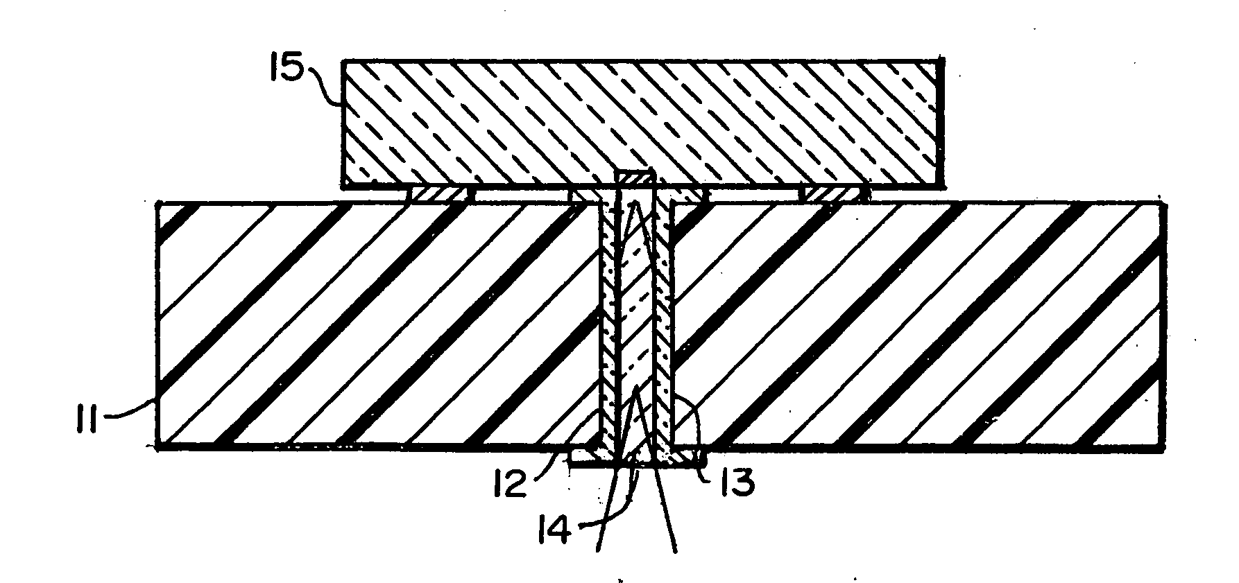
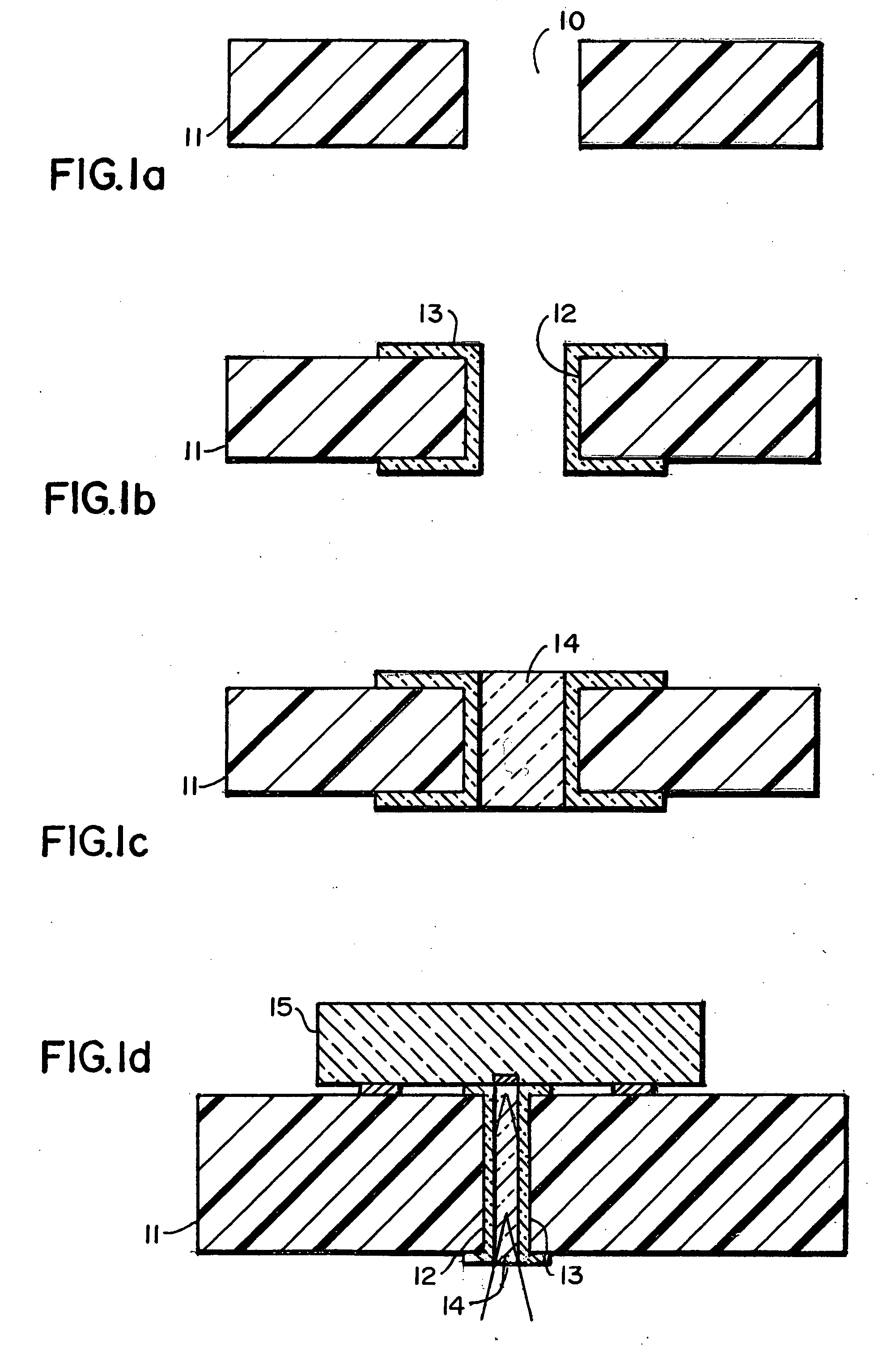
[0018] Referring to the drawings more particularly by reference numbers, sectional side views of process steps sequence to fabricate vertical channel guide optical via are shown in FIGS. 1a-1e. A via 10 may be formed by known processes in a silicon substrate 11 as shown in FIG. 1a.

[0019] While the examples herein disclose silicon as the substrate, other elements / compounds can conveniently form the substrate. For example, in addition to silicon, germanium, indium phosphide, silicon / germanium, gallium arsenide, glass, quartz, sapphire and silicon carbide can be used to form the substrate.

[0020] The thru via 10 shown in FIG. 1a may be formed by first partially etching it in the silicon substrate 11 to the desired depth and later grinding silicon from the backside. Alternatively, the thru via 10 may be formed by completely etching it in the silicon substrate 11. The sidewall 12 of via 10 may be covered with low refractive index material to provide the function of a cladding layer 13 a...


PUM


Abstract

Method of fabricating a semiconductor die with a microlens associated therewith. More particularly, a method for fabricating a vertical channel guide optical via through a silicon substrate wherein the optical via can contain lens elements, a discrete index gradient guiding pillar and other embodiments. Also disclosed are means for transferring, coupling and or focusing light from an electronic-optical device on the top of a semiconductor substrate through the substrate to a waveguiding medium below the substrate. The high alignment accuracies afforded by standard semiconductor fabrication processes are exploited so as to obviate the need for active alignment of the optical coupling or light guiding elements.

Description

FIELD OF THE INVENTION [0001] The present invention relates to a method of fabricating a semiconductor die with a microlens associated therewith. More particularly, the present invention relates to a method for fabricating a vertical channel guide optical via through a silicon substrate wherein the optical via can contain lens elements, a discrete index gradient guiding pillar and other embodiments. BACKGROUND OF THE INVENTION [0002] Optoelectronic systems used for optically communicating between devices typically consist of a driver, an optical light emitting device such as a VCSEL, light coupling elements such as mirrors, gratings and optical waveguides for transporting optical signals from one point to another. An assembly of such optoelectronic system comprises fabricating waveguides and coupling elements on top of a substrate such as a printed wiring board (PWB) and then attaching a VCSEL device on top of such a substrate. The optical light emitted from the VCSEL is coupled int...

Claims


Application Information

Patent Timeline
IPC IPC(8): H01L23/48G02B6/42H05K1/02
CPCH01L23/481H05K1/0274G02B6/43H01L2924/0002H01L2924/00H01L2224/16225
Inventor BUDD, RUSSELL A.CHINIWALLA, PUNIT P.PATEL, CHIRAG S.
Owner GLOBALFOUNDRIES INC
Features
  • Generate Ideas
  • Intellectual Property
  • Life Sciences
  • Materials
  • Tech Scout
  • Unparalleled Data Quality
  • Higher Quality Content
  • 60% Fewer Hallucinations
Learn More