Gain normalization of a digitally controlled oscillator in an all digital phase locked loop based transmitter
a digital control and gain normalization technology, applied in the field of communication, can solve the problems of unplanned loop output perturbation, relativity large latencies, etc., and achieve the effect of reducing complexity, reducing resolution, and high precision multiplication function
- Summary
- Abstract
- Description
- Claims
- Application Information
AI Technical Summary
Benefits of technology
Problems solved by technology
Method used
Image
Examples
first embodiment
Wideband ADPLL: First Embodiment
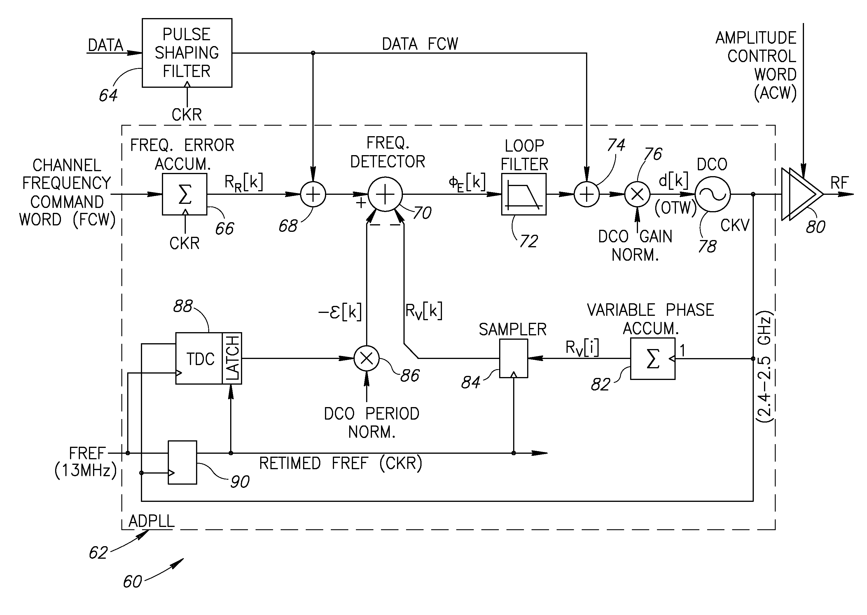
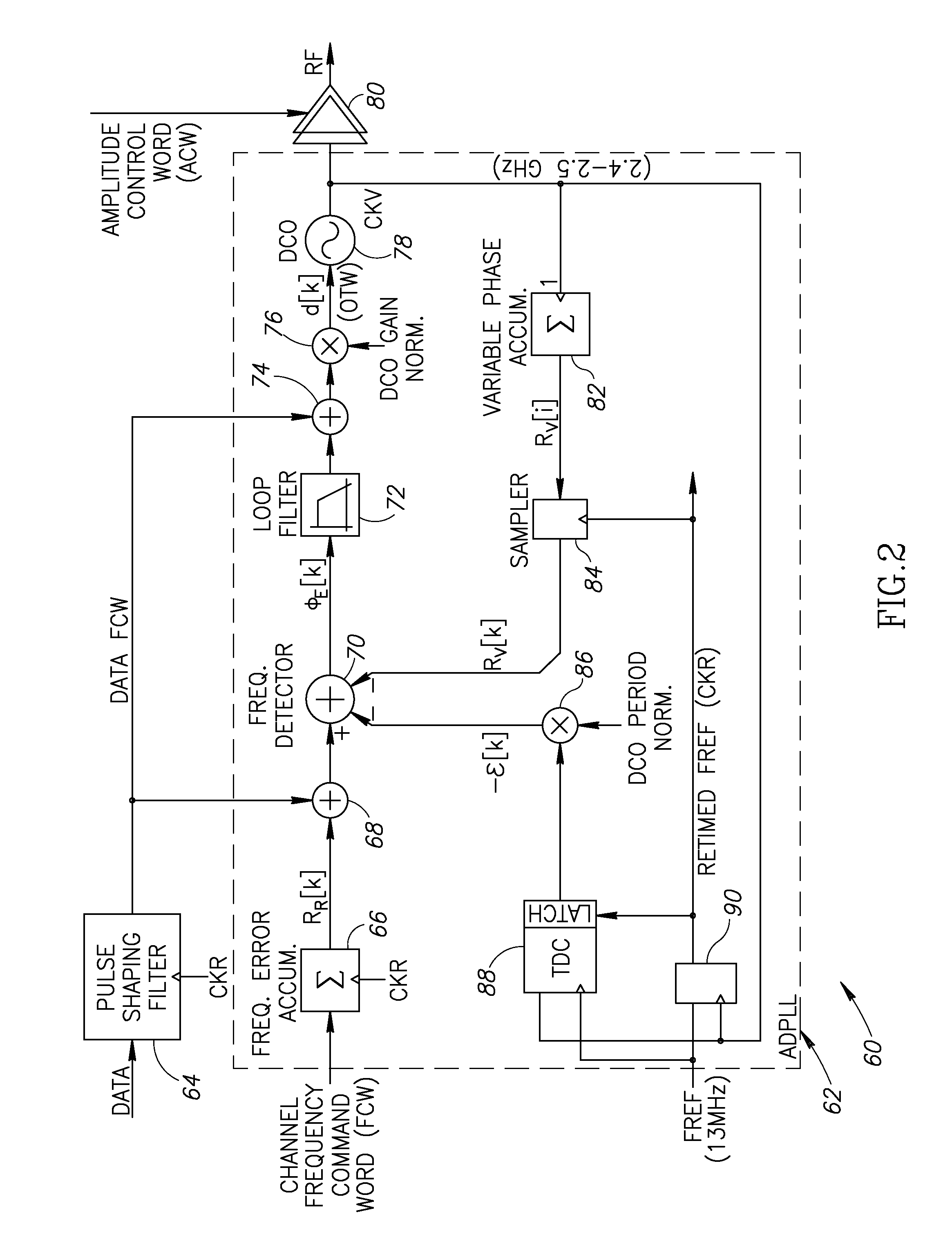
[0031] A block diagram illustrating a first embodiment transmitter based on an all digital phase domain PLL incorporating time to digital converter (TDC) and digitally controlled oscillator (DCO) circuits with wideband frequency modulation capability is shown in FIG. 2. The transmitter, generally referenced 60, comprises pulse shaping filter 64, digital pre-power amplifier 80 and ADPLL 62. The ADPLL comprises a reference phase accumulator 66, adders 68, 74, time to digital converter (TDC) system 88, phase detector 70, loop filter 72, DCO gain normalizer 76, frequency reference retimer 90, sampler 84, DCO period normalization 86 and digitally controlled oscillator (DCO) 78.
[0032] Further details of the operation of the transmitter 60 can be found in U.S. Patent Publication No. 2006 / 0033582A1 and U.S. Patent Publication No. 2006 / 0038710A1 cited supra. The frequency reference (FREF) clock contains the only reference timing information for the RF frequen...
second embodiment
Wideband ADPLL: Second Embodiment
[0039] In accordance with the invention, a DCO gain normalization mechanism that overcomes these disadvantages is provided. A block diagram illustrating a second embodiment DRP transmitter based on an all digital PLL and incorporating the gain normalization mechanism of the present invention is shown in FIG. 4. The transmitter, generally referenced 120, comprises complex pulse shaping filter 122, amplitude modulation block 124, low and high band digital pre-power amplifiers 142, 144, respectively, and ADPLL 121. The transmitter is operative to perform quadrature modulation in the polar domain in addition to the generation of the local oscillator (LO) signal for the receiver. Almost all clocks in the system are derived directly from this source. Note that the transmitter is constructed using digital techniques that exploit the high speed and high density of the advanced CMOS, while avoiding problems related to voltage headroom. The ADPLL circuit 121 r...
third embodiment
Wideband ADPLL: Third Embodiment
[0060] A block diagram illustrating the phase modulation path of a third embodiment transmitter is shown in FIG. 6. The baseband multi-data rate data path 191 comprises adder 200, delay registers 201, 192, 194, 196, 198, 206, 210, re-sampler or data rate converter 212 and multiplier 204 and gain normalization 208 for full bit multiplying the data by a high precision modulation path multiplier 207. The ADPLL loop 190 comprises phase accumulator / detector system 214, loop gain normalization 216 for multiplying a low precision loop multiplier 215, adder 220, registers 218, 222, clock edge dividers 226, 228, 230, frequency reference resampling registers 232, 234 and DCO 224.
[0061] The Figure illustrates the phase / frequency modulation path in the third generation DRP (i.e. third embodiment). It adds support for the high data rates of the WCDMA and WLAN standards by dramatically increasing the frequency modulating bandwidth. The maximum bandwidth limitation...
PUM
 Abstract
Description
Claims
Application Information
 - R&D
- Intellectual Property
- Life Sciences
- Materials
- Tech Scout
- Unparalleled Data Quality
- Higher Quality Content
- 60% Fewer Hallucinations
Browse by: Latest US Patents, China's latest patents, Technical Efficacy Thesaurus, Application Domain, Technology Topic, Popular Technical Reports.
© 2025 PatSnap. All rights reserved.Legal|Privacy policy|Modern Slavery Act Transparency Statement|Sitemap|About US| Contact US: help@patsnap.com


