Apparatus for etching wafer by single-wafer process and single wafer type method for etching wafer

Inactive Publication Date: 2007-04-19
SUMCO CORP
View PDF2 Cites 15 Cited by
  • Summary
  • Abstract
  • Description
  • Claims
  • Application Information

AI Technical Summary

Benefits of technology

[0028] As explained above, according to the present invention, the etching fluid flowing down over the edge portion of the wafer placed on the wafer-chuck is blown off in the outward radial direction away from the wafer by injection of a gas from the gas injection device, the etching fluid blown off by the gas injection device is aspirated together with a gas by the first fluid-aspirating device, and the etching fluid blown off by the gas injection device or scattered by the centrifugal force is aspirated together with the gas by the second fluid-aspirating unit. Because of such a constitution, most of the etching fluid is scattered outside of the wafer by a centrifugal force which accompanies the rotation of the wafer, and a part of the etching fluid which tends to pass round the edge portion of the wafer towards the undersurface of the wafer is blown off in the outward radial direction away from the wafer by a high speed gas flow generated by the gas injection device. Then, the above-described scattered etching fluid is aspirated by the second fluid-aspirating device, and the above-described blown off etching fluid is aspirated by the first fluid-aspirating device, or otherwise, scattered outside of the wafer and is aspirated by the second fluid-aspirating device. As a result, etching fluid is prevented from passing round towards the undersurface of the wafer. Since the scattered etching fluid does not adhere to the upper surface of the wafer again, the upper surface of the wafer can be homogeneously etched. In addition, since the etching fluid is retained at the edge portion of the wafer only for a short duration, localized deformation of the edge portion can be effectively inhibited.
[0033] When the gas supply unit is activated and the compressed gas passes through the injection channel and is injected from the injection nozzle, by providing the injection nozzle with an annular peak protruding so as to narrow the opening of the injection nozzle, it is possible to enhance a flow rate of gas flow flowing, in the clearance between the upper surface of the wafer-chuck and undersurface of the wafer, in the outward radial direction away from the wafer.
[0035] In addition, by blowing off the etching fluid flowing down over the edge portion of the wafer placed on the wafer-chuck by the gas injection device, and by aspirating the etching fluid scattered by a centrifugal force caused by the rotation of the wafer and the above-described blown off etching fluid, the same in the above-described constitution, it is possible to prevent the etching fluid from passing round towards the undersurface of the wafer. In addition, since the scattered etching fluid does not adhere to the upper surface of the wafer again, the upper surface of the wafer can be homogeneously etched. Moreover, since the etching fluid is retained at the edge portion of the wafer only for a short duration, localized deformation of the edge portion can be effectively inhibited.

Problems solved by technology

During the manufacturing process of semiconductor devices, the damaged layer of the wafer induces crystal defects such as slip dislocations to occur, and thereby deteriorating the mechanical strength of the wafer and causing adverse effects on the electrical property of the wafer.
However, there is a possibility that the etching fluid stays for a long duration at the peripheral portion of the wafer causing undesirable etching of the edge portion subjected to the staying etching fluid.
In addition, in the conventional single-wafer type processing apparatus described in the above-described Patent Document 1, there is a possibility that the gas supplied to the space below the wafer scatters the etching fluid.

Method used


Image

  • Apparatus for etching wafer by single-wafer process and single wafer type method for etching wafer
  • Apparatus for etching wafer by single-wafer process and single wafer type method for etching wafer
  • Apparatus for etching wafer by single-wafer process and single wafer type method for etching wafer

Examples


first embodiment

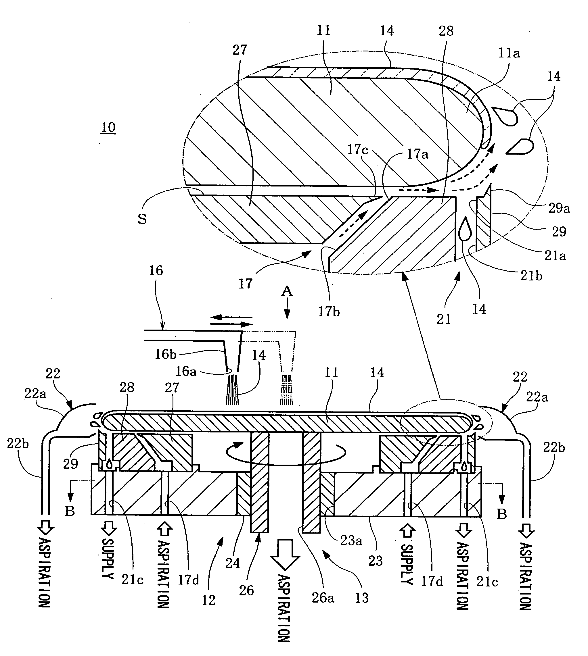
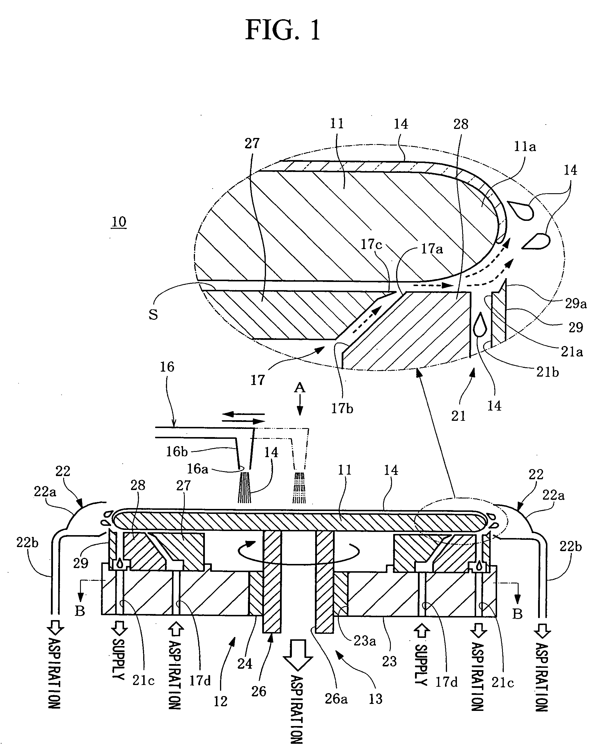
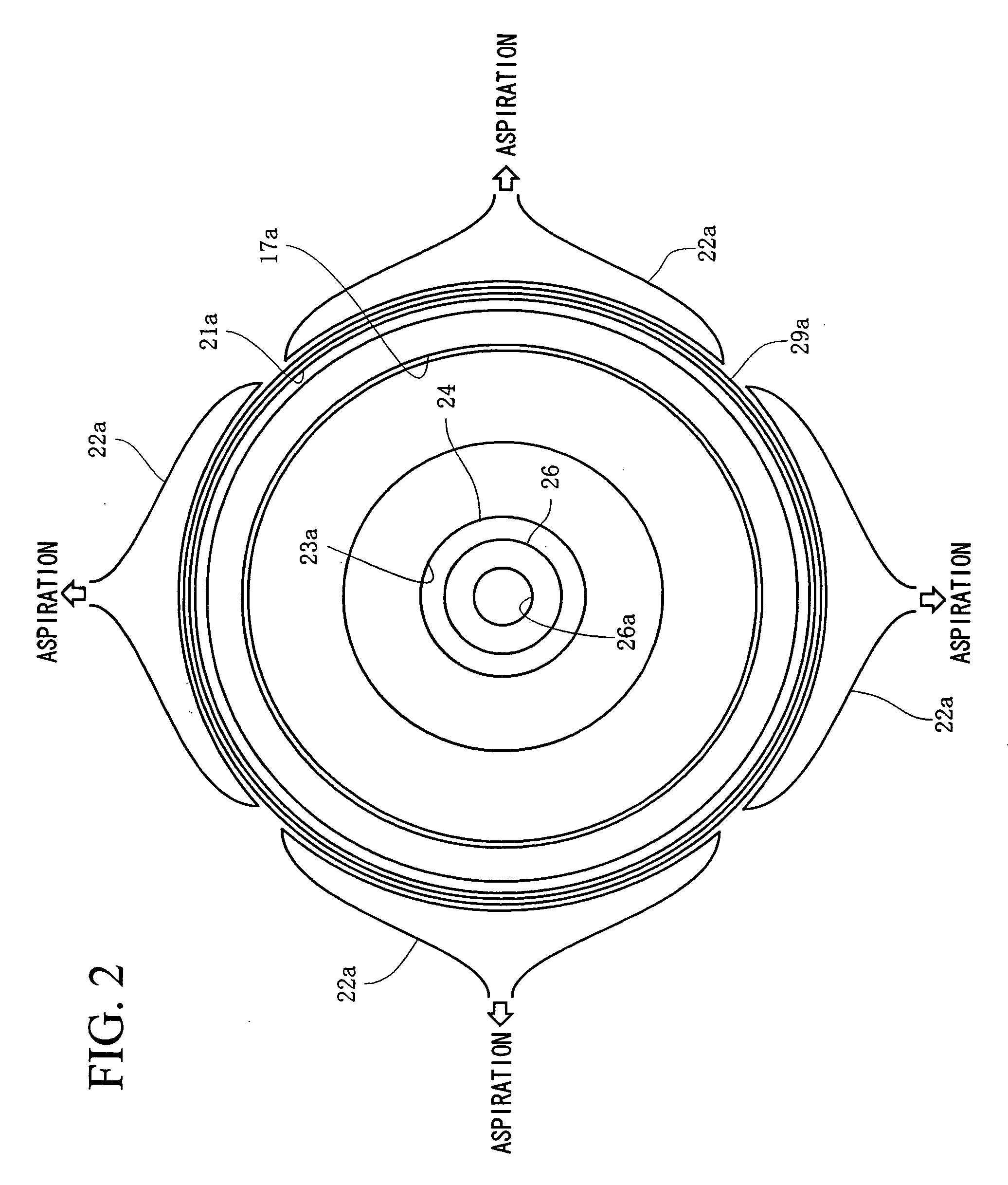
[0040] As shown in FIG. 1, a single-wafer processing apparatus 10 for etching a single silicon wafer 11 is received in a chamber and comprises: a wafer-chuck 12 which mounts the single silicon wafer 11 having a thin disk shape and horizontally supports the wafer 11; a rotation unit 13 for rotating the wafer about the vertical center axis of the wafer 11; an etching fluid supply device 16 for supplying etching fluid 14 to the upper surface of the wafer 11 mounted on the wafer-chuck; a gas injection device 17 which blows off the etching fluid 14 flowing over an edge portion 11a of the wafer 11 in the outward radial direction away from the wafer 11; a first fluid-aspirating device 21 and a second fluid-aspirating device 22 that aspirate both of the etching fluid 14 scattered by a centrifugal force which accompanies the rotation of the wafer 11, and the etching fluid 14 blown off by the gas injection device 17. The wafer 11 is sliced from a silicon single crystal ingot. A circumference ...


PUM

PropertyMeasurementUnit
Diameteraaaaaaaaaa
Circumferenceaaaaaaaaaa

Abstract

An apparatus for etching a wafer by a single-wafer process comprises a fluid supplying device which feeds an etching fluid on a wafer, and a wafer-chuck for horizontally holding the wafer. The wafer-chuck is equipped with a gas injection device for injecting a gas to the wafer, a first fluid-aspirating device, and a second fluid-aspirating device. The etching fluid supplied on the wafer is spread by a rotation of the wafer. The etching fluid is scattered by a centrifugal force, or flows down over an edge portion of the wafer and is blown-off by the gas injected from the gas injection unit, and is aspirated by the first fluid-aspirating device or the second fluid-aspirating device.

Description

BACKGROUND OF THE INVENTION [0001] 1. Field of the Invention [0002] The invention relates to an apparatus for etching a wafer while horizontally holding a single wafer and rotating the wafer. Priority is claimed on Japanese Patent Application No. 2005-302538, filed Oct. 18, 2005, the content of which is incorporated herein by reference. [0003] 2. Description of Related Art [0004] Generally, a manufacturing process of semiconductor wafers comprises: slicing a wafer from a single crystal ingot; facing and mechanically grinding (lapping) the wafer; etching the wafer; mirror polishing (polishing) the wafer; and cleaning the wafer. Through such steps, wafers having highly flat surfaces are manufactured. During the manufacturing process, a wafer is subjected to various mechanical workings such as cutting a block from the ingot, grinding the outside cylindrical surface of the block, slicing the wafer from the block, and lapping the wafer. As a result, the upper side of the wafer includes a...

Claims


Application Information

Patent Timeline
IPC IPC(8): C03C15/00H01L21/306H01L21/302
CPCH01L21/67075H01L21/6708Y10S134/902H01L21/3063
Inventor KOYATA, SAKAEHASHII, TOMOHIROMURAYAMA, KATSUHIKOTAKAISHI, KAZUSHIGEKATOH, TAKEO
Owner SUMCO CORP
Why Eureka
Try Eureka