Photoactive component with organic layers

a technology of organic materials and components, applied in the field of photoactive components with organic layers, can solve the problems of insufficient high fields, inability to use mono-crystalline organic materials, and inability to produce multiple layers with sufficient structural perfection, etc., and achieve the effect of reducing recombination losses

Active Publication Date: 2007-04-26
HELIATEK GMBH
View PDF5 Cites 109 Cited by
  • Summary
  • Abstract
  • Description
  • Claims
  • Application Information

AI Technical Summary

Benefits of technology

[0029] The invention is therefore based on the task of extensively reducing recombination losses or the occurrence of inactive areas in solar cells with organic layers.

Problems solved by technology

In organic solar cells, sufficiently high fields are not available, with the result that all concepts for organic cells promising success are based on exciton separation at photoactive interfaces.
For large-area applications, however, the use of mono-crystalline organic materials is not possible and the production of multiple layers with sufficient structural perfection has so far proved to be very difficult.
Despite the advantages described with interpenetrating networks, a critical issue lies in the fact that closed transport paths for both electrons and holes to their respective contacts have to be present in the mixed layer.
Furthermore, as the individual materials only fill a part of the mixed layer, the transport properties for the charge carriers deteriorate significantly in comparison to the pure layers.
Moreover, organic dyes only exhibit individual absorption bands, with the result that a material can never cover the complete optical spectrum.
If, like Yakimov, we apply these recombination centers directly onto the photoactive material, they will not only ensure the required recombination of charge carriers from the n-th cell with opposite charge carriers from the n+1-th cell, but also form undesired recombination centers for excitons or charge carrier pairs from one and the same cell.
Either recombination losses or inactive areas result from this.
Such a problem occurs analogously in individual diode structures.
In this way, however, the recombination losses occur immediately at the transition zones between the active layer and contact electrode.

Method used


Image

  • Photoactive component with organic layers
  • Photoactive component with organic layers
  • Photoactive component with organic layers

Examples


Embodiment Construction

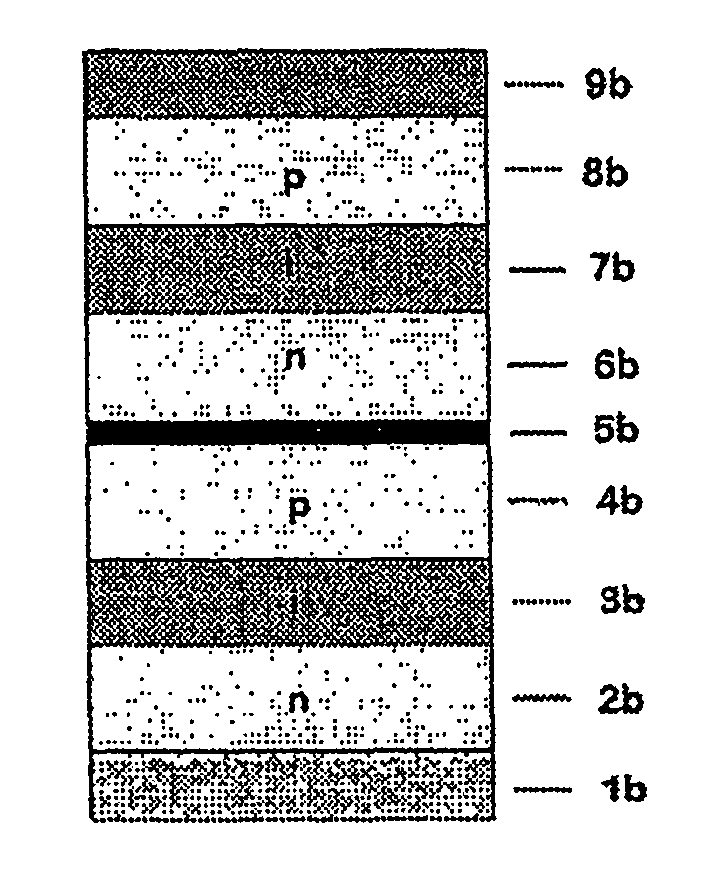
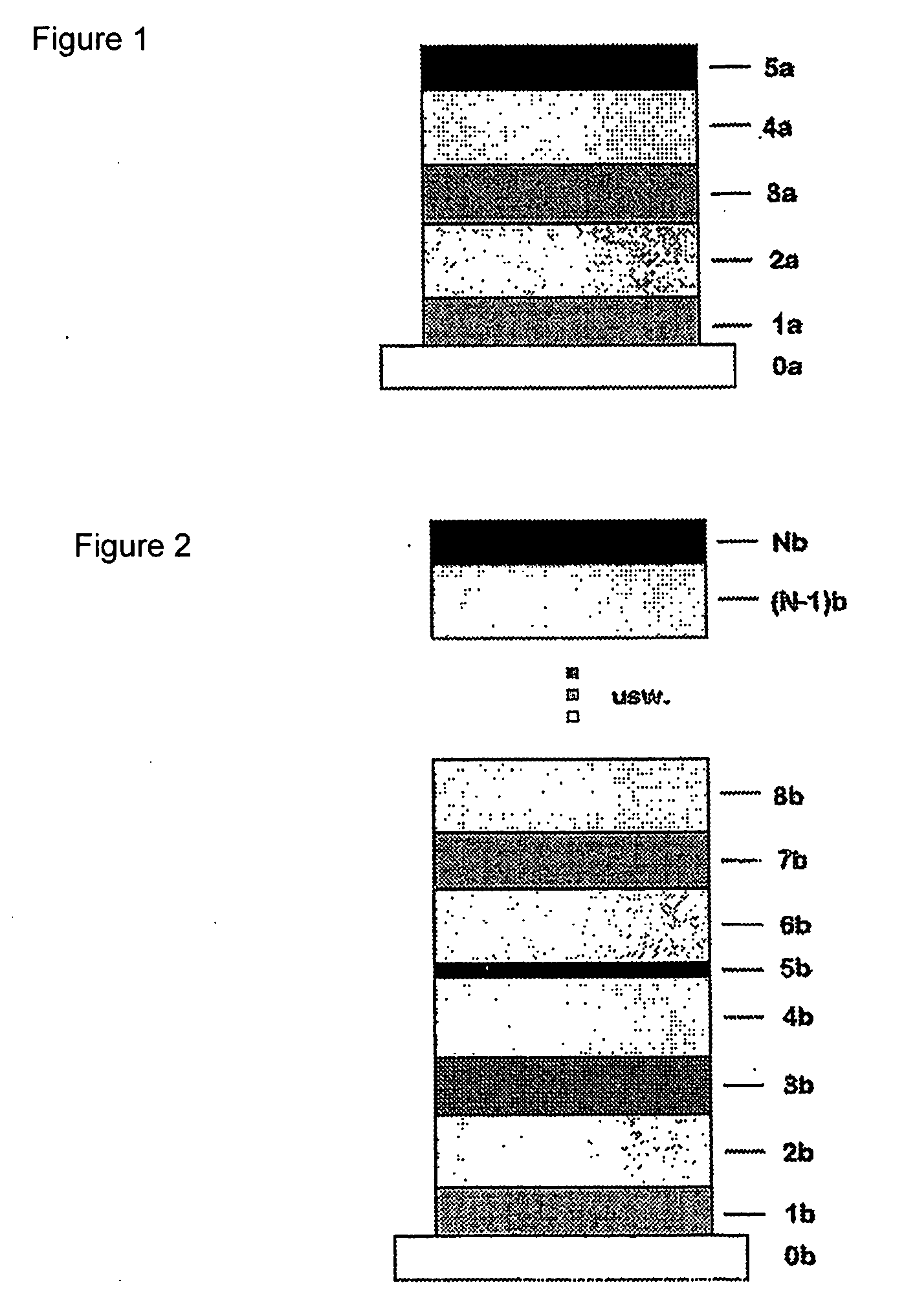
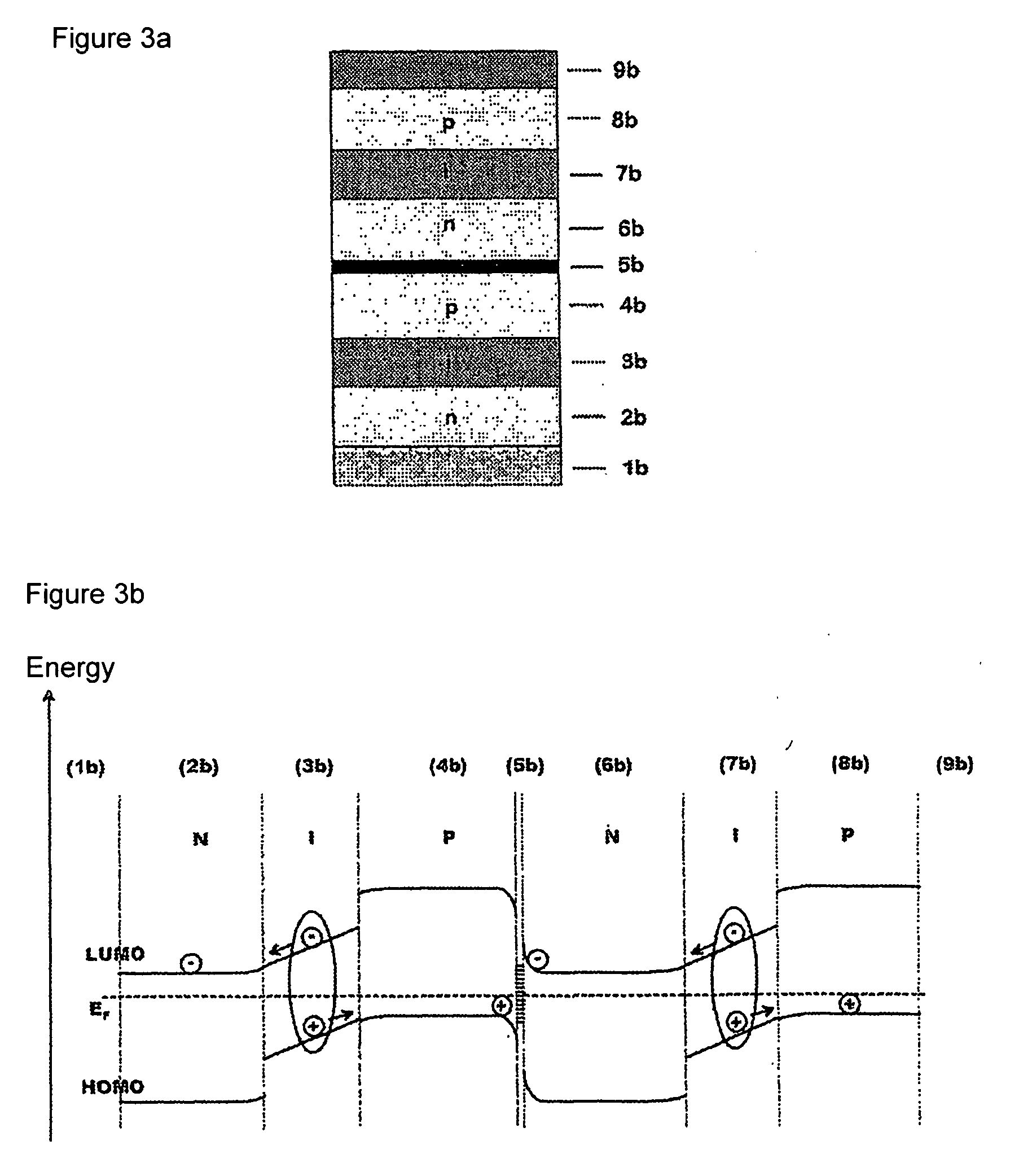
[0051] An advantageous embodiment shown in FIG. 1 comprising a structure for an organic solar cell corresponding to the invention according to the principle of an individual diode structure contains the following layers: [0052]0a.) Carrier, substrate, [0053]1a.) Base contact, mostly transparent, with optional organic or inorganic contact-making layer [0054]2a.) Charge carrier transport layer (wide-gap), p-doped or n-doped [0055]3a.) Active layer [0056]4a.) Charge carrier transport layer (wide-gap), n-doped or p-doped [0057]5a.) Top contact, optionally including organic or inorganic contact-making layer.

[0058] In accordance with this, the component advantageously consists of a pin or nip layer structure. The pin (or nip) structure for its part consist of two or more organic charge carrier transport layers respectively (2a and 4a) and a layer system (3a ) located between the organic layer (2a) and the organic layer (4a), in which the light is absorbed. Furthermore, the complete struc...


PUM

PropertyMeasurementUnit
optical absorption coefficientsaaaaaaaaaa
thickaaaaaaaaaa
thickaaaaaaaaaa

Abstract

The invention relates to a photoactive component, especially a solar cell, comprising organic layers and formed by at least one stacked pi, ni, and/or pin diode. The diodes are characterised in that they comprise at least one p-doped or n-doped transport layer having a larger optical band gap than that of the photoactive layer. The individual diodes are characterised by a high internal quantum yield, but can be optically thin (peak absorption <80%). A high external quantum yield is obtained by either enlarging the optical path of the incident light in the diodes using light traps, or by stacking a plurality of the diodes. The transition between two diodes being facilitated by transition layers for the purposes of improved recombination and generation. Both forms of embodiment have a number of specific advantages using the doped transport layers with a large band gap.

Description

CROSS REFERENCE TO RELATED APPLICATIONS [0001] This application is a 371 filing of PCT International application no. PCT / DE2004 / 000574 filed Mar. 19, 2004 and published in German as WO 2004 / 083958 A2 on Sep. 30, 2004 which claims priority of German application no. 103 13 232.5 filed Mar. 19, 2003, the disclosures of which are hereby incorporated by reference herein in their entirety.BACKGROUND ART [0002] The invention concerns a photoactive component with organic layers, in particular a solar cell, consisting of a series of organic thin layers and contact layers with a doped transport layer and a photoactive layer, arranged in a pi, ni, or pin diode structure from a p, i or n layer respectively. [0003] Since the demonstration of the first organic solar cell with an efficiency in the percentage range by Tang et al. 1986 [C. W. Tang et al. Appl. Phys. Lett. 48, 183 (1986)], organic materials have been intensively examined for various electronic and optoelectronic components. Organic s...

Claims


Application Information

Patent Timeline
Patent Type & Authority Applications(United States)
IPC IPC(8): H01L33/00G03F1/00H01L27/30H01L31/00H01L31/101H01L51/00H01L51/30
CPCB82Y10/00H01L27/302H01L51/002H01L51/0046H01L51/0059H01L51/0078H01L51/0092H01L51/424H01L51/4253H01L51/4293H01L2251/308Y02E10/549H10K30/57H10K71/30H10K85/211H10K85/311H10K85/631H10K85/381H10K30/20H10K30/40H10K30/30H10K2102/103H10K30/00
Inventor DRECHSEL, JENSPFEIFFER, MARTINMAENNIG, BERTLEO, KARL
Owner HELIATEK GMBH
Why Eureka
Try Eureka