Structure and method of molded QFN device suitable for miniaturization, multiple rows and stacking

a technology of qfn devices and molded components, which is applied in the direction of semiconductor devices, semiconductor/solid-state device details, electrical devices, etc., can solve the problems of difficult to reduce fabrication costs, the height of the device has not yet reached the desired thin profile, and the existing cavity-down package is difficult to achieve. , to achieve the effect of high speed performance, excellent thermal device performance, and increased density of bonding pads or solder lands

Active Publication Date: 2007-04-26
TEXAS INSTR INC
View PDF2 Cites 72 Cited by
  • Summary
  • Abstract
  • Description
  • Claims
  • Application Information

AI Technical Summary

Benefits of technology

[0013] The copper chip pad of the devices made according to the invention can be soldered to a heat sink for excellent thermal device performance. The wire connection can be kept to a minimum, holding electrical resistance and inductance to a small value for high speed performance. The devices can be made so that they will be not much thicker than the thickness of the silicon chip even for multi-row designs.
[0014] The devices according to the invention provide many variations. For instance, other metals than copper or copper alloys may be used as starting sheets; an example is aluminum. The metal of the sacrificial layers may also be varied. The adhesion between the encapsulation compound and the metal cuboids may be strengthened by chemical or plasma means. The density of bonding pads or solder lands can be increased without much difficulty. The overall methodology is tolerant for changes in device type or size, without substantial increase in fabrication cost.

Problems solved by technology

These packages have an outline adding less than 20% to the chip area; however, their height has not yet reached the desired thin profile.
In the wire ball-bonding process, however, the mechanically weak heat-affected zone of the wire necessitates the vertical position of the wire over the ball, leading to the hallmark high looping of wire bonding.
The height required by the wire looping and the design of the multi-layer package are hindrances for achieving a thin device profile; in addition, they are not amenable to lowering the fabrication cost.
It is difficult in existing cavity-down packages to bring heat-conducting metal pieces into contact with the semiconductor chip.
It is also difficult to lay out short, high-speed, or shielded, lines in multi-layer packages, given the technical constraints of wire bonding and multi-layer package construction.

Method used


Image

  • Structure and method of molded QFN device suitable for miniaturization, multiple rows and stacking
  • Structure and method of molded QFN device suitable for miniaturization, multiple rows and stacking
  • Structure and method of molded QFN device suitable for miniaturization, multiple rows and stacking

Examples


Embodiment Construction

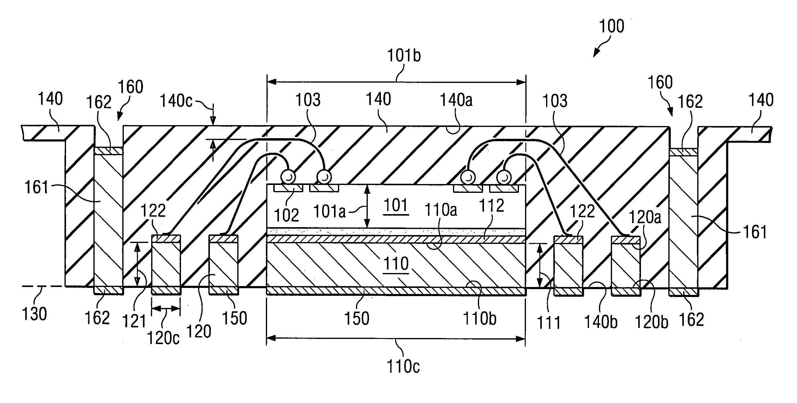
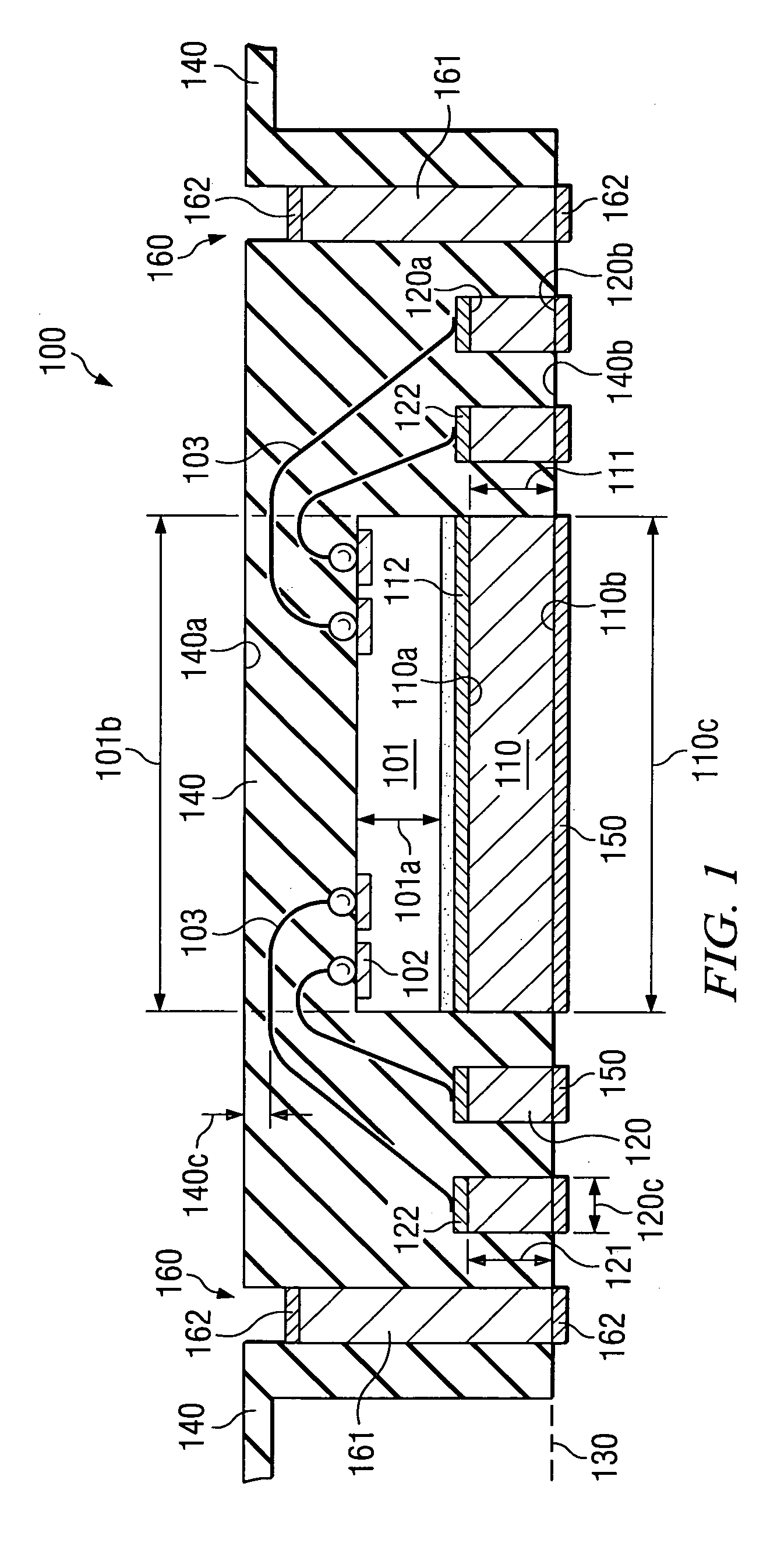
[0026]FIG. 1 shows a semiconductor device example, a representative of the Quad Flat Pack no-Lead (QFN) family, which has been designed and fabricated by the concepts of the invention. The device is generally designated 100. In the device is a semiconductor chip 101, which has a thickness 101a, a length 101b, a width (not shown in FIG. 1), and a plurality of bond pads 102. The market offers a wide selection of chip sizes 101 for QFN devices; a typical example is a chip of 2.4 mm by 1.65 mm; other chips may be smaller or much larger. The size and number of bond pads 102 also varies widely; the number, for instance, from 8 to 44. As an example, the chip just quoted has 10 bond pads, each pad the size 0.275 mm by 0.35 mm. The chip thickness 101a also varies considerably; in some devices, the thickness is 275 μm, in other devices only 100 μm.

[0027] In the device is further a first cuboid 110 made of metal. A preferred choice of metal is copper or a copper alloy; alternative choices are ...


PUM


Abstract

A semiconductor device comprising a semiconductor chip (101) assembled on a first copper cuboid (110); the cuboid has sides of a height (111). The device further has a plurality of second copper cuboids (120) suitable for wire bond attachment; the second cuboids have sides of a height (121) substantially equal to the height of the first cuboid. The back surfaces of all cuboids are aligned in a plane (130). Encapsulation compound (140) is adhering to and embedding the chip, the wire bonds, and the sides of all cuboids so that the compound forms a first surface (140b) aligned with the plane of the back cuboid surfaces and a second surface (140a) above the embedded wires. For devices intended for stacking, the devices further comprise a plurality of vias (160) through the encapsulation compound from the first to the second compound surfaces; the vias are filled with copper, and the via locations are matching between the devices-to-be-stacked.

Description

FIELD OF THE INVENTION [0001] The present invention is related in general to the field of semiconductor devices and more specifically to low-profile, chip-scale stacked packages and method for fabrication. DESCRIPTION OF THE RELATED ART [0002] The strong market trend for consumer products such as mobile phones and other portable, hand-held and wearable products demands semiconductor devices as building blocks, which consume only little area and height, when mounted onto circuit boards. One of the most successful approaches for slim, small-size semiconductor devices has been the development of so-called “chip-scale packages”. These packages have an outline adding less than 20% to the chip area; however, their height has not yet reached the desired thin profile. [0003] A widely practiced methodology of assembling and enclosing a semiconductor chip begins with providing a “cavity down” package and assembling the chip in the cavity. The assembly process includes the step of attaching th...

Claims


Application Information

Patent Timeline
Patent Type & Authority Applications(United States)
IPC IPC(8): H01L23/12H01L21/60H01L23/49
CPCH01L21/4828H01L21/568H01L21/6835H01L24/45H01L24/48H01L24/85H01L25/105H01L2224/32245H01L2224/45015H01L2224/45144H01L2224/48091H01L2224/48095H01L2224/48247H01L2224/48465H01L2224/48599H01L2224/73265H01L2924/01005H01L2924/01011H01L2924/01013H01L2924/01014H01L2924/01028H01L2924/01029H01L2924/01033H01L2924/01046H01L2924/01047H01L2924/0105H01L2924/01078H01L2924/01079H01L2924/01082H01L2924/014H01L2924/15331H01L2924/20752H01L2924/30107H01L2924/3025H01L2924/00014H01L2924/01006H01L2924/00H01L24/83H01L2225/1029H01L2224/85H01L2225/1058H01L2924/00012H01L2924/10253H01L2224/83H01L2224/48511H01L2924/181H01L24/73H01L2224/85439H01L2224/05599
Inventor ABBOTT, DONALD C.
Owner TEXAS INSTR INC
Why Eureka
Try Eureka