Nitride semiconductor device

a technology of nitride and semiconductor, which is applied in the direction of semiconductor lasers, semiconductor devices, electrical apparatus, etc., can solve the problems of low p-type impurity rate of nitride semiconductor, increased manufacturing cost, and difficult resistance reduction, and achieve excellent esd tolerance

Active Publication Date: 2007-05-03
NICHIA CORP
View PDF8 Cites 104 Cited by
  • Summary
  • Abstract
  • Description
  • Claims
  • Application Information

AI Technical Summary

Benefits of technology

[0026] According to the present invention, uneven distribution of the electric current in the p-side nitride semiconductor layer ...

Problems solved by technology

That is, although the p-side nitride semiconductor layer in the nitride semiconductor device shows the p-type conductivity through doping with a p-type impurity such as Mg, an activation rate of the p-type impurity in the nitride semiconductor is low so that it is difficult to reduce the resistance thereof.
In addition, when the p-side nitride semiconductor layer is formed too thick, it may lead deterioration in the crystallinity and increase in the manufacturing cost so that there is a limitation in increasing the thickness of the layer.
Therefore, sufficient in-plane distribution of the electri...

Method used


Image

  • Nitride semiconductor device
  • Nitride semiconductor device
  • Nitride semiconductor device

Examples


embodiment 1

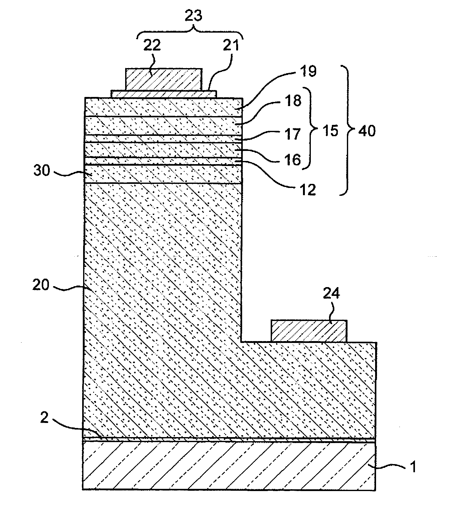
[0034]FIG. 1 is a schematic cross-sectional view showing a nitride semiconductor device (light emitting diode) according to Embodiment 1 of the present invention. A buffer layer 2, an n-side nitride semiconductor layer 20, an active layer 30, a p-side nitride semiconductor layer 40 are stacked on a foreign substrate 1 such as sapphire. Also, as the p-side nitride semiconductor layer 40, a p-side wide band gap layer 12, a first p-side nitride semiconductor layer 16, a second p-side nitride semiconductor layer 17, a third p-side nitride semiconductor layer 18, and a p-side contact layer 19 are stacked in the order. An n-side pad electrode 24 is disposed on a surface of the n-side nitride semiconductor layer 20, which is exposed by removing the p-side nitride semiconductor layer 40 and an active layer 30 partially. A p-side ohmic electrode 21 and the p-side pad electrode 22, which are collectively called a “p-side electrode 23” are disposed on the p-side contact layer 19 in the p-side ...

embodiment 2

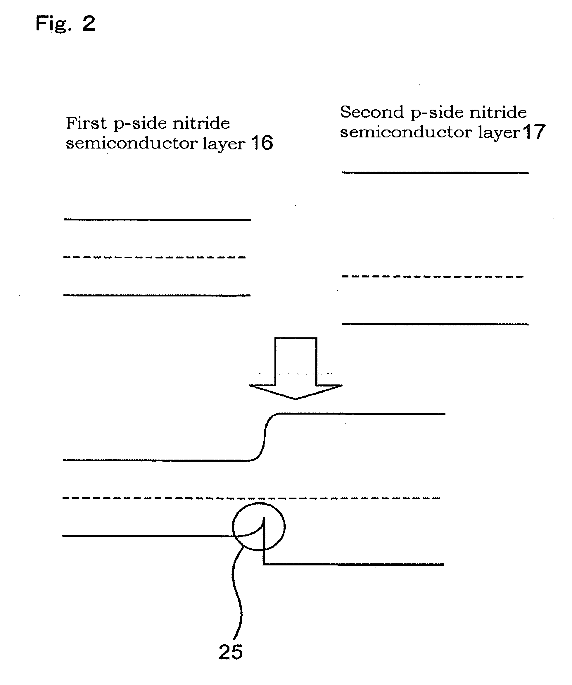
[0096]FIG. 3 is a schematic cross-sectional view showing a nitride semiconductor device according to Embodiment 2. In Embodiment 2, an intermediate layer 14 is provided between the first p-side nitride semiconductor layer 16 and the p-side wide band gap layer 12. Other respects are similar to that shown in Embodiment 1.

[0097] The intermediate layer 14 plays such a role as the buffer layer, by preventing the p-type impurity diffused from the wide band gap layer 12 from infiltrating deeply into the nitride semiconductor layer 16. By providing such intermediate layer 14, the p-type impurity concentration in the first p-side nitride semiconductor layer 16 can be reduced and the mobility of the hole accumulation region 25 can further be elevated. Consequently, the p-type impurity concentration in the intermediate layer 14 is adjusted to be at least lower than that in the p-side wide band gap layer 12. The p-type impurity concentration in the intermediate layer 14 is desirably from 5×101...

embodiment 3

[0098]FIG. 4 is a schematic cross-sectional view showing a nitride semiconductor device according to Embodiment 3. In Embodiment 3, the three-layer structure is stacked multiple times repeatedly. Other respects are similar to that shown in Embodiment 1. That is, as shown in FIG. 4, after stacking a p-side wide band gap layer 12 on an active layer 30, a first p-side nitride semiconductor layer 16, a second p-side nitride semiconductor layer 17, and a third p-side nitride semiconductor layer 18 are stacked as a first set of a three-layer structure 15. Then, the first p-side nitride semiconductor layer 16′, the second p-side nitride semiconductor layer 17′, and the third p-side nitride semiconductor layer 18′ are stacked as a second set of the three-layer structure 15′. After repeating such stacking for a necessary number of times, a p-side contact layer 19 is formed.

[0099] As shown in the present embodiment, by stacking the three-layer structure 15 repeatedly, electric current diffus...


PUM


Abstract

A nitride semiconductor device having excellent ESD tolerance, by preventing uneven distribution of the electric current in the p-side nitride semiconductor layer. The p-side nitride semiconductor layer (40) comprises, from the active layer (30) side, (a) a p-side wide band gap layer (12) containing a p-type impurity and (b) a three-layer structure (15) comprising a first p-side nitride semiconductor layer (16), a second p-side nitride semiconductor layer (17), and a third p-side nitride semiconductor layer (18).

Description

BACKGROUND OF THE INVENTION [0001] 1. Field of the Invention [0002] The present invention relates to a nitride semiconductor device employing a nitride semiconductor (for example, InaAlbGa1-a-bN, 0≦a, 0≦b, a+b≦1) used in a light emitting device such as a light emitting diode (LED) and a laser diode (LD), in a photodetector such as a solar cell and an optical sensor, and in an electric device such as a transistor and a power device. [0003] 2. Discussion of the Related Art [0004] A nitride semiconductor device is utilized in a light emitting device such as a light emitting diode (LED) and a laser diode (LD), in a photodetector such as a solar cell and an optical sensor, and in an electric device such as a transistor and a power device. Especially, a nitride semiconductor has been widely utilized in an optical device such as a light emitting diode (LED) and a laser diode (LD). A nitride semiconductor device as an optical device generally has a double hetero structure in which an active...

Claims


Application Information

Patent Timeline
IPC IPC(8): H01L29/06H01L33/02H01L33/14H01L33/32
CPCH01L29/2003H01L29/205H01L33/02H01L33/14H01L33/32H01S5/3054H01S5/3211H01S5/32341
Inventor SANGA, DAISUKEKASAI, HISASHIMIYAGI, KAZUHIRO
Owner NICHIA CORP
Why Eureka
Try Eureka