FinFET transistor fabricated in bulk semiconducting material

a technology of semiconducting materials and transistors, which is applied in the direction of semiconductor devices, basic electric elements, electrical appliances, etc., can solve the problems of reducing the ability of the gate to control whether, ensuring a fully depleted channel region becomes increasingly difficult, and the conventional mosfet suffers from several problems, so as to facilitate the formation of finfet devices, the effect of high uniformity and reproducibility

Inactive Publication Date: 2007-05-10
ATMEL CORP
View PDF9 Cites 36 Cited by
  • Summary
  • Abstract
  • Description
  • Claims
  • Application Information

AI Technical Summary

Benefits of technology

[0006] A field effect transistor (FET) device structure and method for forming FETs for scaled semiconductor devices is presented. Specifically, FinFET devices described are fabricated from bulk semiconductor wafers, as opposed to silicon-on-insulator (SOI) or separation by implantation of oxygen (SIMOX) wafers, in a highly uniform and reproducible manner. The method facilitates formation of FinFET devices from readily-available bulk semiconductor substrates with improved and reproducible fin height control while providing isolation between source and drain regions of the FinFET device.

Problems solved by technology

As MOSFETs are scaled to channel lengths below about 100 nm, conventional MOSFETs suffer from several problems.
In particular, interactions between the source and drain of the MOSFET degrade an ability of the gate to control whether the device is on or off.
As device size is scaled, however, ensuring a fully depleted channel region becomes increasingly difficult, since the distance between the source and drain is reduced.
The reduced distance results in an increased interaction with the channel thus reducing gate control and increasing short channel effects.
Additional significant unsolved problems remain with the aforementioned electronic devices.
In addition to the increased area required, the body contact problem has prevented the semiconductor industry from using FinFET devices for nonvolatile memory due to current processing complications in making the contact.
However, the Fried et al. method requires careful control of a silicon etch depth in the bulk wafer, a “damaging process” in areas of silicon surrounding the fin, oxidation of the damaged areas, and a fin oxidation process to thin the fin to a required level.
Each of these processes require tremendous process control and are likely non-manufacturable in a production environment.

Method used


Image

  • FinFET transistor fabricated in bulk semiconducting material
  • FinFET transistor fabricated in bulk semiconducting material
  • FinFET transistor fabricated in bulk semiconducting material

Examples


Embodiment Construction

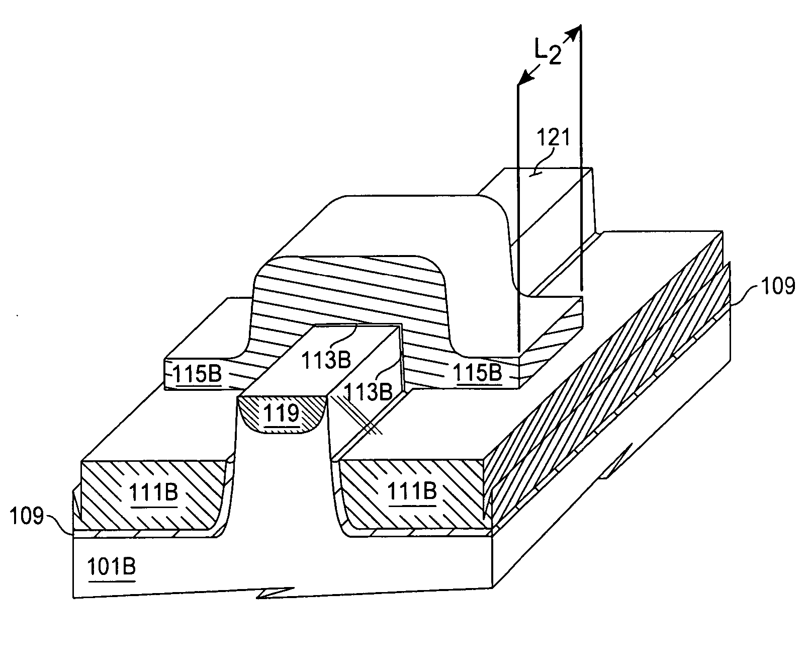
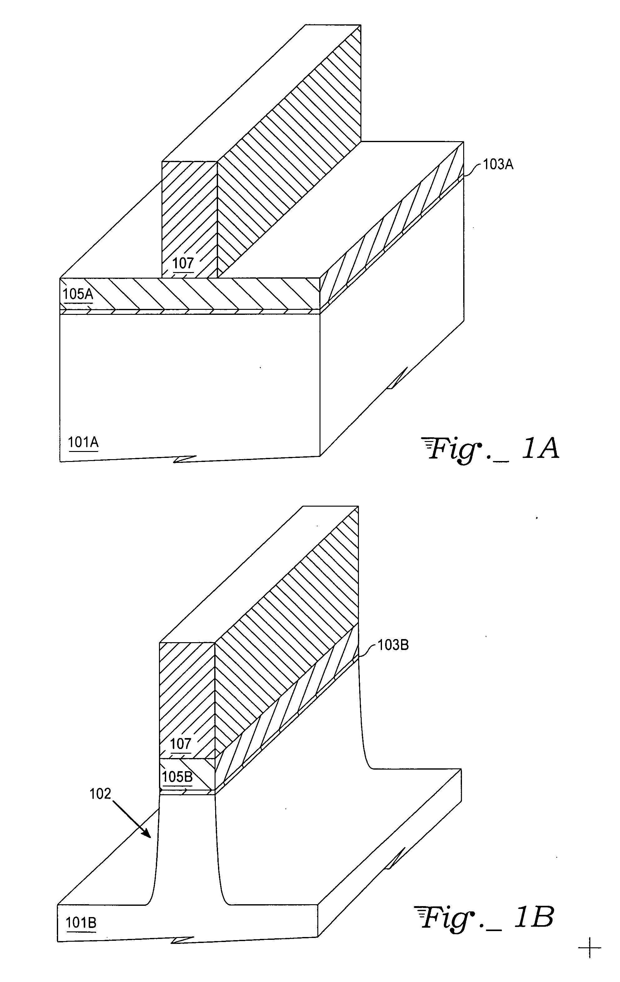
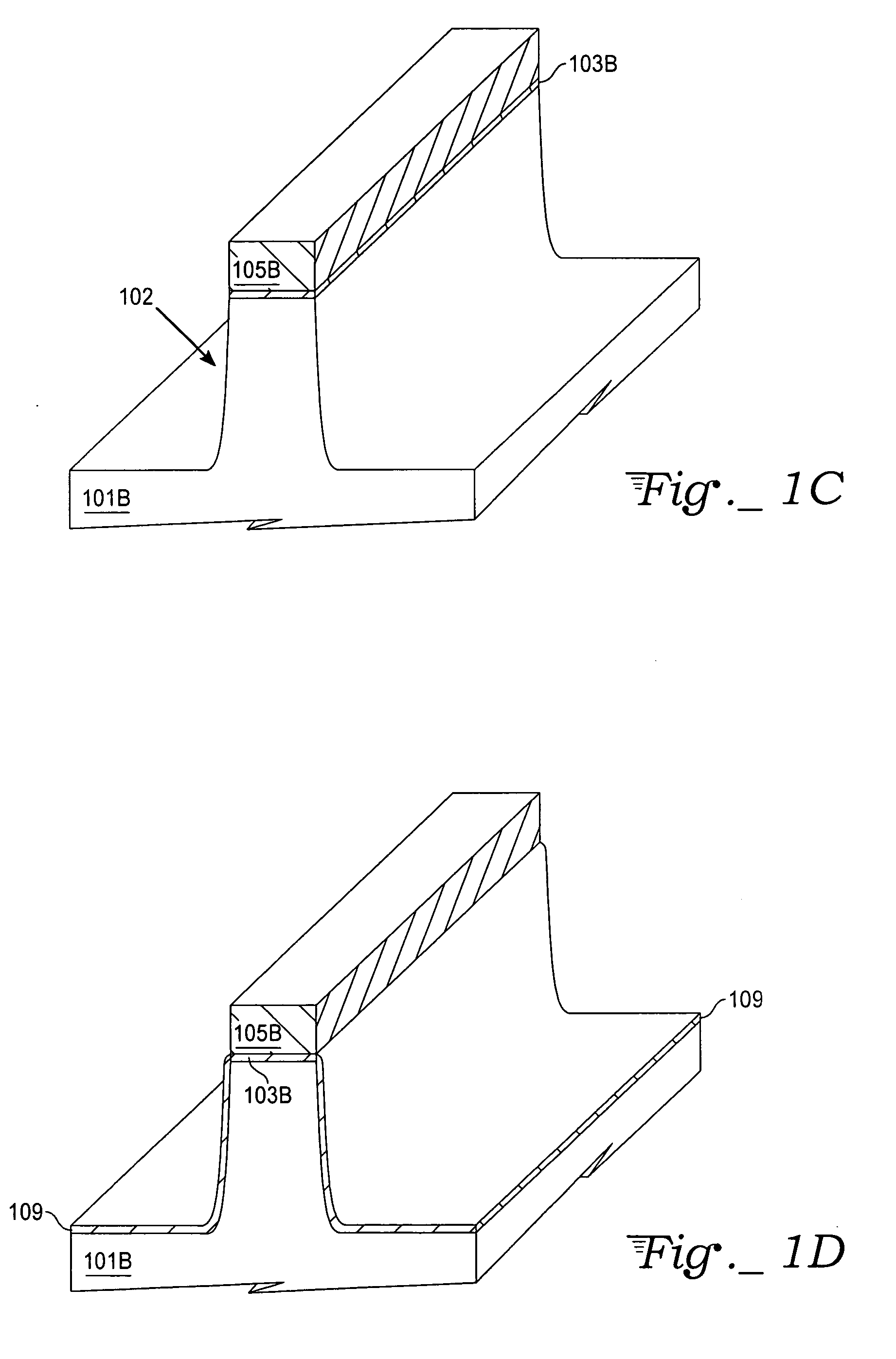
[0010] With reference to FIG. 1A, a substrate 101A has a thin silicon dioxide layer 103A, a thicker silicon nitride layer 105A, and a patterned photoresist mask layer 107. In a specific exemplary embodiment, the substrate 101A is be a silicon wafer. However, a skilled artisan will recognize that other semiconductor materials may be used instead of silicon for the substrate 101A. Other semiconductor materials include, for example, elemental semiconductors such as germanium, compound semiconductors such as group III-V, and II-VI materials, and semiconducting alloys. If elemental semiconductors other than silicon, or compound semiconductors are employed, an atomic layer deposition (ALD) process may be employed for producing thin, high quality oxide layers.

[0011] The silicon dioxide layer 103A is a pad oxide to prevent thermally-induced stresses from developing between particular dissimilar materials, such as between silicon and the silicon nitride layer 105A. The silicon dioxide layer...


PUM


Abstract

A field effect transistor (FET) device structure and method for forming FETs for scaled semiconductor devices. Specifically, FinFET devices are fabricated from bulk semiconductor wafers, as opposed to silicon-on-insulator (SOI) or separation by implantation of oxygen (SIMOX) wafers, in a highly uniform and reproducible manner. The method facilitates formation of FinFET devices from readily-available bulk semiconductor substrates with improved and reproducible fin height control while providing isolation between source and drain regions of the FinFET device.

Description

TECHNICAL FIELD [0001] The present invention relates generally to FET and MOSFET transistors, and more particularly the invention relates to field effect transistors having channel regions extending vertically from a supporting substrate between horizontally disposed source and drain regions. BACKGROUND ART [0002] Metal-oxide-semiconductor field effect transistor (MOSFET) technology is a dominant electronic device technology in use today. Performance enhancement between generations of devices is generally achieved by reducing an overall size of the device, resulting in an enhancement in device speed. This size reduction is generally referred to as device scaling. As MOSFETs are scaled to channel lengths below about 100 nm, conventional MOSFETs suffer from several problems. In particular, interactions between the source and drain of the MOSFET degrade an ability of the gate to control whether the device is on or off. The degradation in control ability phenomenon is called a short-cha...

Claims


Application Information

Patent Timeline
Patent Type & Authority Applications(United States)
IPC IPC(8): H01L29/76
CPCH01L29/66795H01L29/7851
Inventor LOJEK, BOHUMIL
Owner ATMEL CORP
Why Eureka
Try Eureka