Manufacturing method of semiconductor device and semiconductor device

a manufacturing method and technology of semiconductor devices, applied in the direction of printed circuit manufacturing, printed circuit aspects, non-metallic protective coating applications, etc., can solve the problems of degrading the sorbability of vacuum adsorption nozzles, hard surface of sealing resins, etc., and achieve satisfactory mounting

Inactive Publication Date: 2007-05-10
RENESAS TECH CORP
View PDF3 Cites 9 Cited by
  • Summary
  • Abstract
  • Description
  • Claims
  • Application Information

AI Technical Summary

Benefits of technology

[0032] Advantageous effects obtained by representative ones of the inventions disclosed in the present application will be explained in brief as follows:
[0033] (1) A resin layer formed by printing of a silicone resin is subjected to defoaming processing and curing processing (bake processing) after its printing. A heavy substance such as a filler contained in a resin at the defoaming processing long in processing time sinks from the upper surface side to the wiring board side at its lower surface. As a result, the surface of the resin layer is brought to a layer of a resin component hard to tear off. Thus, a compression force merely acts on the layer of the resin component in the surface layer of the resin layer even if the wiring board is divided, in the case of such a division that the wiring board is folded back to the resin layer side. Therefore, the resin portion remains without the division of the wiring board (non-divided resin portion remains). In the dividing method according to the present invention, a wiring board formed of ceramic is forced up (upper swing) by means of a lower clamp claw of a clamper, and some of a protruded wiring board portion that protrudes from a conveying chute is pressed against a support body to carry out a first division under bending stress. Thereafter, the upward-located clamper is rotatably swung (lower swing) downward to allow an upper clamp claw to press down the protruded wiring board portion, thereby performing a reverse division at the first division section again as a second division. Since the second division allows a tensile force to act on a remaining and thin non-divided resin portion, the non-divided resin portion is torn off. Thus, the perfect division is enabled. Fractionalizing is done by a one-row division and an individual division so that each semiconductor device is manufactured.
[0034] (2) A pickup mechanism, which conveys products brought to semiconductor devices by being fractionized, vacuum-adsorbs and holds a semiconductor device at a final stage by a tool but measures the degree of vacuum in its held state. Then, the pickup mechanism is controlled based on information about the degree of vacuum. When the measured degree of vacuum is greater than or equal to the reference degree of vacuum, the pickup mechanism conveys the semiconductor devices to the corresponding non-defective product storage unit. When the degree of vacuum is less than the reference degree of vacuum, the pickup mechanism conveys the semiconductor devices to the corresponding defective product storage unit. Thus, only products in each of which the flatness of the surface of an encapsulating body is satisfactory, can be shipmented. As a result, the pickup of each semiconductor device is done reliably upon the work of mounting of the semiconductor device by a user, thus making it possible to carry out satisfactory mounting.

Problems solved by technology

The patent document 1 has pointed out that a problem arises in that when the sealing resin is formed by a potting method, the surface of the sealing resin is hard to be flattened, and when a semiconductor device manufactured as a result thereof is surface-mounted to a circuit substrate, sorbability based on a vacuum adsorption nozzle is degraded.

Method used


Image

  • Manufacturing method of semiconductor device and semiconductor device
  • Manufacturing method of semiconductor device and semiconductor device
  • Manufacturing method of semiconductor device and semiconductor device

Examples


first preferred embodiment

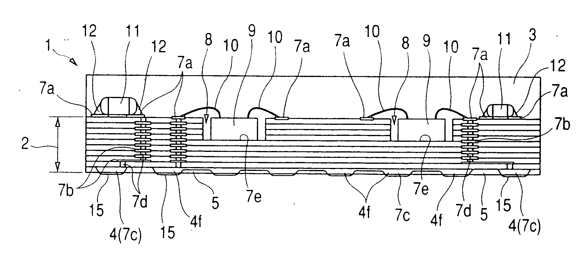
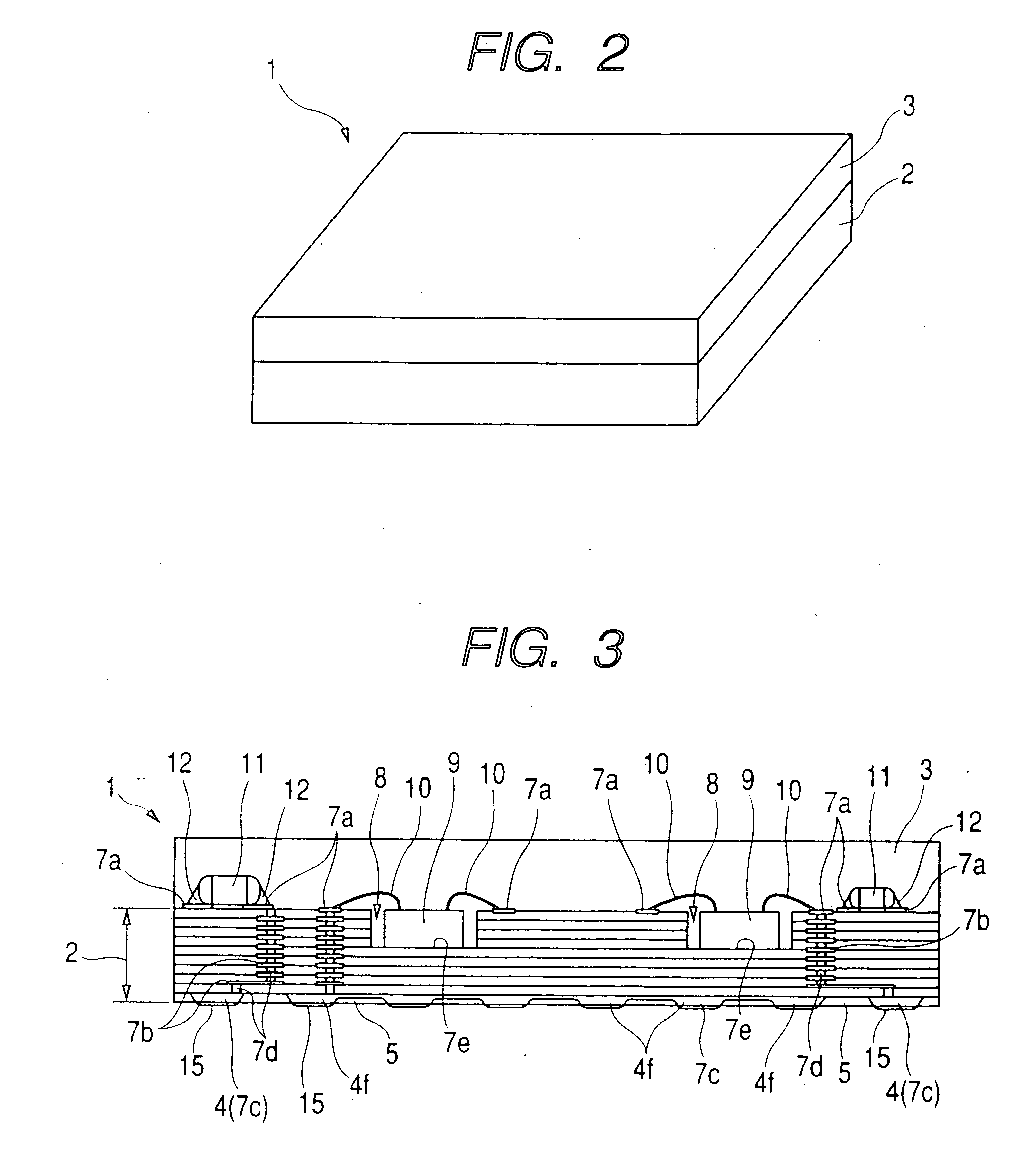
[0070] The first embodiment will explain an example in which the present invention is applied to the manufacture of a semiconductor device (hybrid integrated circuit device) built in a cellular phone. FIGS. 1 through 29 are drawings related to a method of manufacturing a semiconductor device, showing the first embodiment of the present invention, and a semiconductor manufacturing apparatus. FIGS. 2 through 7 are drawings related to the semiconductor device manufactured by the first embodiment. FIGS. 1(a) to 1(c) and FIGS. 8 through 29 are drawings related to the semiconductor manufacturing apparatus.

[0071] As shown in FIG. 2, the semiconductor device (hybrid integrated circuit device) 1 manufactured by the semiconductor device manufacturing method according to the present embodiment comprises, in appearance, a module substrate 2 constituted of a square-shaped low temperature calcined laminated substrate, and an encapsulator or encapsulating body 3 formed of an insulating resin that...

second preferred embodiment

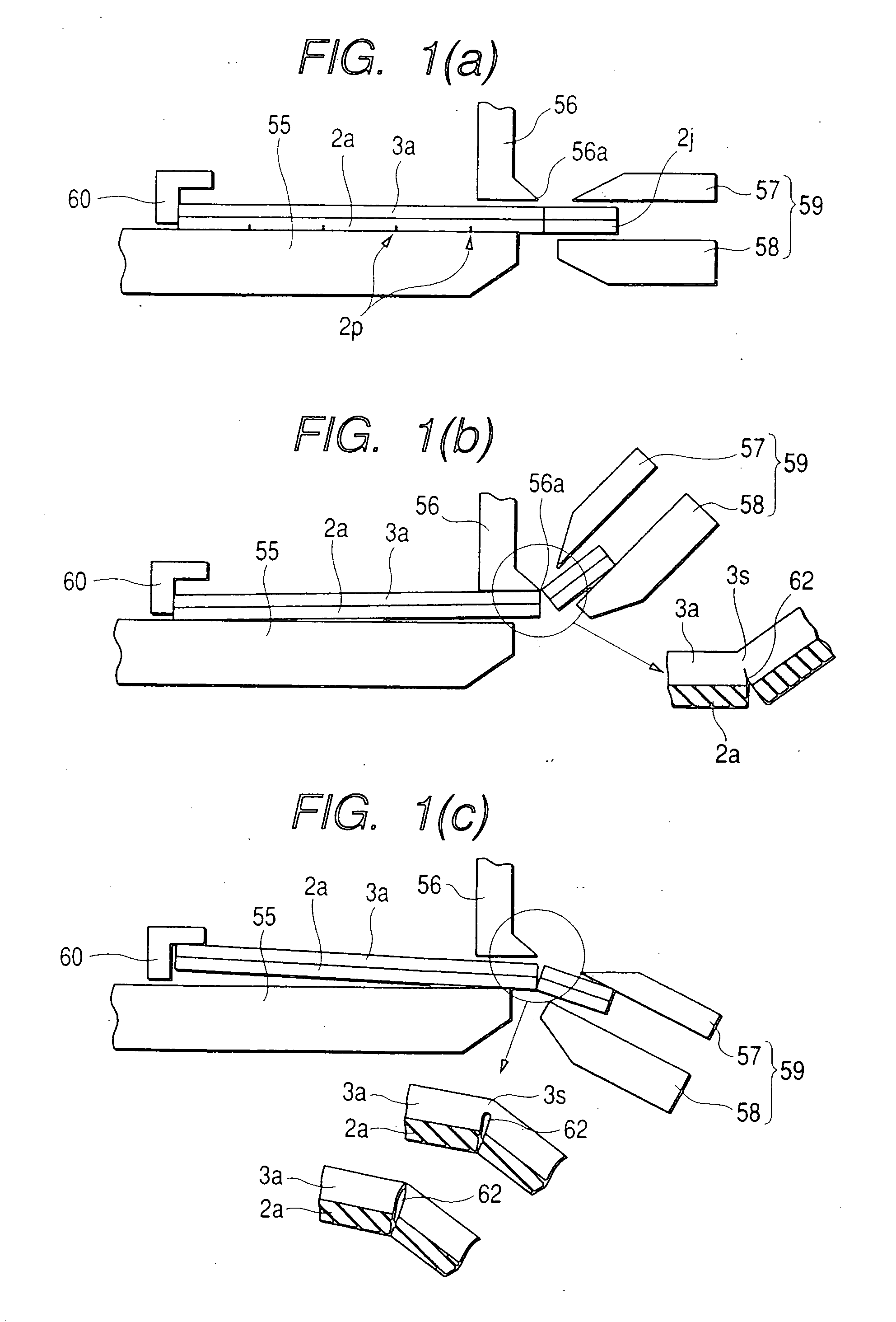
[0174] A second embodiment shows an example in which in a semiconductor manufacturing apparatus, the division of a wiring board is made satisfactory and the position to divide the wiring board can be set accurately. FIGS. 30(a) and 30(b) is a typical view illustrating a cutting mechanism for cutting a substrate covered with a resin layer and its cut state.

[0175] As described in the first embodiment, the surface of the resin layer 3a formed by printing is low in flatness due to an undulation or the like. When the undulation is large, a resin layer 3a is not brought into contact with a fulcrum 56a of a support body 56 when a protruded wiring board portion 2j of a substrate 2a is forced up, and a top portion 142 of an undulation 141 comes into contact with the lower surface of the support body 56, as shown in FIG. 31. It has turned out that since the position to which a dividing force is applied, does not correspond to the position of the fulcrum 56a in such a case, the division does ...


PUM


Abstract

In a dividing method according to the present invention, a wiring board formed of ceramic is forced up (upper swing) by a lower clamp claw of a clamper, and some of a protruded wiring board portion protruding from a conveying chute is pressed against a support body to perform a first division under bending stress. Thereafter, the upward-located clamper is rotatably swung (lower swing) downward to allow an upper clamp claw to press down the protruded wiring board portion, thereby performing a reverse division at the first division section again as a second division. Since the second division allows a tensile force to act on a remaining and thin non-divided resin portion, the non-divided resin portion is torn off. Thus, the perfect division is enabled. Fractionalizing is done by a one-row division and an individual division so that each semiconductor device is formed.

Description

CROSS-REFERENCE TO RELATED APPLICATION [0001] The present application claims priority from Japanese patent application No. 2003-367435 filed on Oct. 28, 2003, the content of which is hereby incorporated by reference into this application. BACKGROUND OF THE INVENTION [0002] The present invention relates to a method of manufacturing a semiconductor device such as a hybrid integrated circuit device (hybrid IC) and a semiconductor manufacturing apparatus, and to, for example, a technique effective if applied to the manufacture of a semiconductor device built in a cellular phone. [0003] As one manufacturing method of a semiconductor device such as a hybrid integrated circuit device, there is known, for example, a technique for mounting a bare chip and other parts over unit sections of a package base substrate, which can be taken or picked up in multi form, thereafter sealing the bare chip and other parts with an insulating resin to form a sealing resin and then cutting the package base s...

Claims


Application Information

Patent Timeline
Patent Type & Authority Applications(United States)
IPC IPC(8): H01L21/00H01L23/28H01L21/44H01L21/48H01L21/50H01L21/56H05K1/03H05K3/00H05K3/28
CPCH01L21/481H01L2224/48227H01L2924/01078H01L2924/01079H01L2924/15153H01L2924/1517H01L2924/19041H01L2924/30107H01L2924/3011H05K1/0306H05K3/0052H05K3/284H05K2201/09036H05K2201/0909H05K2203/302H01L2924/181H01L2924/00012
Inventor KOBAYASHI, YOSHIHIKOSATO, SUSUMUTANIMOTO, KOKIYAMADA, TOMIONAKAJIMA, HIROKAZUKUDAISHI, TOMOAKISHIOKAWA, YOSHINORINIITSU, TOSHIHARUIDA, TSUTOMU
Owner RENESAS TECH CORP
Why Eureka
Try Eureka