

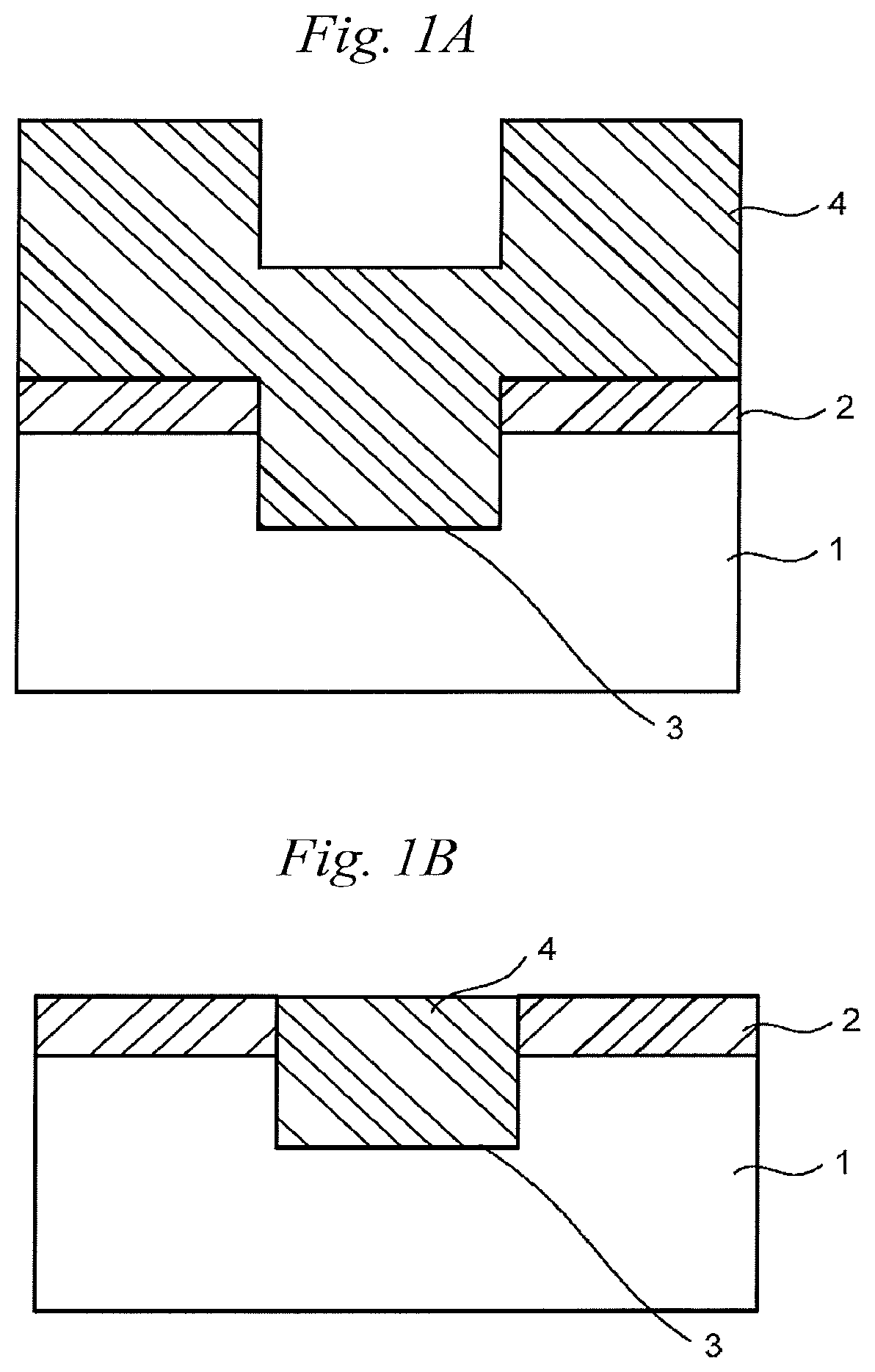
Polishing agent, polishing method, and liquid additive for polishing
a technology of polishing agent and polishing method, which is applied in the direction of polishing compositions, other chemical processes, lapping machines, etc., can solve the problems of insufficient removal rate of silicon nitride films, and achieve low removal rate, high selection ratio, and high removal rate
- Summary
- Abstract
- Description
- Claims
- Application Information
AI Technical Summary
Benefits of technology
Problems solved by technology
Method used
Image

Examples
examples
The present invention is specifically described below by reference to working examples and comparative examples, but the invention should not be construed as being limited to those examples.
examples 1 to 15
are working examples, and Examples 16 to 20 are comparative examples. In the following examples, unless otherwise indicated, “%” means “mass %”. Characteristic values were measured and evaluated by the following methods.
pH
The pH was measured using a pH meter MH-30R manufactured by DKK-TOA Corporation.
Average Secondary Particle Size
The average secondary particle size was measured using a laser diffraction / scattering particle size distribution analyzer (manufactured by Horiba, Ltd., device name: LA-920).
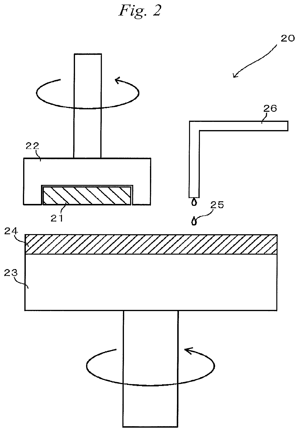
Polishing Characteristics
The polishing characteristics were evaluated by performing polishing using a fully automatic CMP polishing device (manufactured by Applied Materials, device name: Mirra). Two-layer pad (VP-3100 manufactured by Dow) was used as the polishing pad, and CVD diamond pad conditioner (manufactured by 3M, trade name: Trizact B5) was used for conditioning the polishing pad. The polishing conditions were polishing pressure: 21 kPa, the number of rotations of polishing pl...
example 1
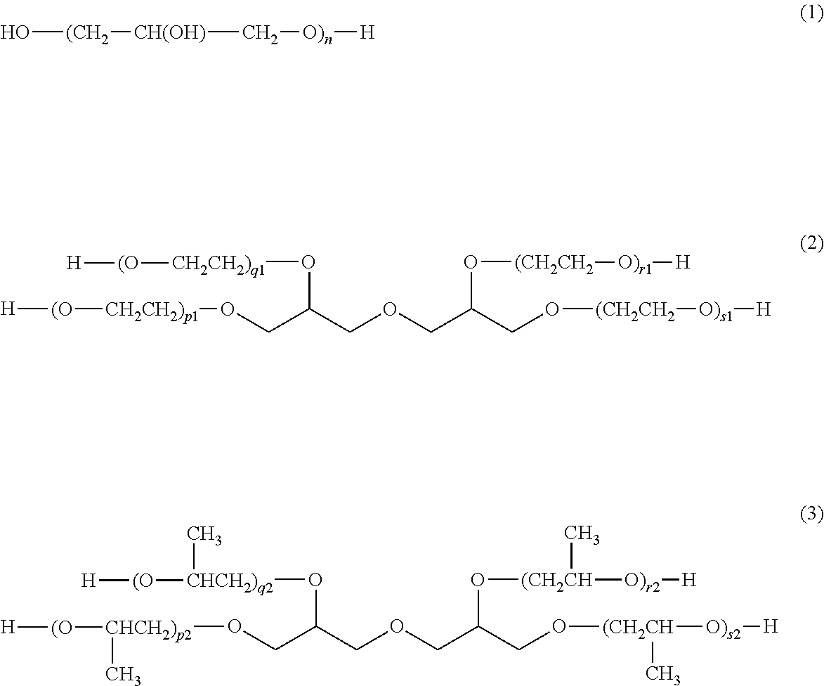
A cerium oxide dispersion (hereinafter referred to as cerium oxide dispersion a) obtained by dispersing cerium oxide particles having an average secondary particle size of 120 nm in pure water was added to pure water such that the content ratio (concentration) of the cerium oxide particles was 0.25% based on the total mass of a polishing agent, and tetrahydrofuran-2-carboxylic acid (hereinafter referred to as “THF-C”) as an organic acid having a monodentate ligand and polyoxyethylene diglyceryl ether (trade name: SC-E750, manufactured by Sakamoto Yakuhin Kogyo Co., Ltd., p1+q1+r1+s1=about 13 in the formula (2), weight average molecular weight: 750) (hereinafter referred to as nonionic polymer A. Shown as “Polyoxyethylene diglyceryl ether (Mw 750)” in Table 1. Mw means a weight average molecular weight.) as a polymer (2) were then added to the dispersion such that the content ratio (concentration) of THF-C was 0.10% and the content ratio (concentration) of the nonionic polymer A was ...
PUM
| Property | Measurement | Unit |
|---|---|---|
| particle size | aaaaa | aaaaa |
| particle size | aaaaa | aaaaa |
| particle size | aaaaa | aaaaa |
Abstract
Description
Claims
Application Information