

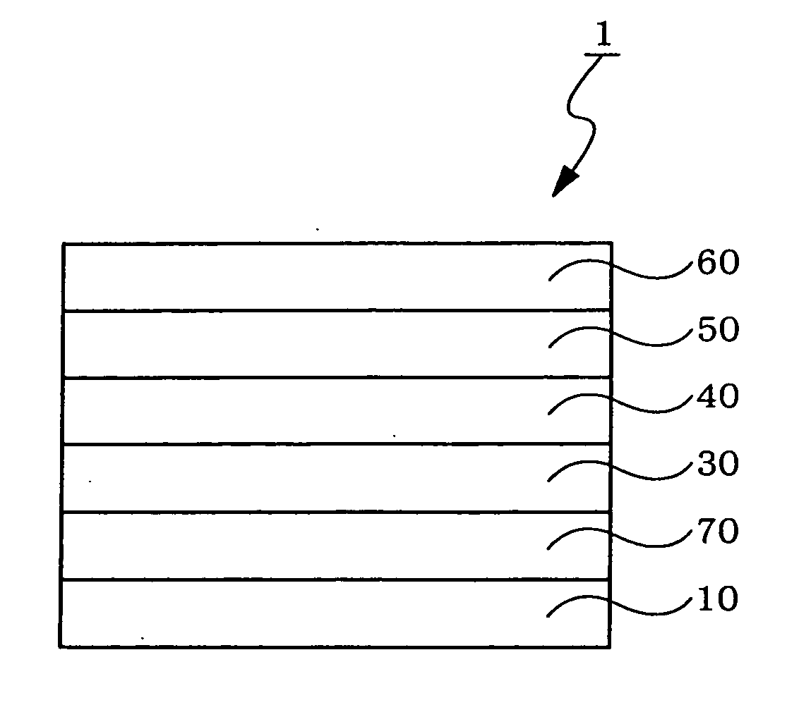
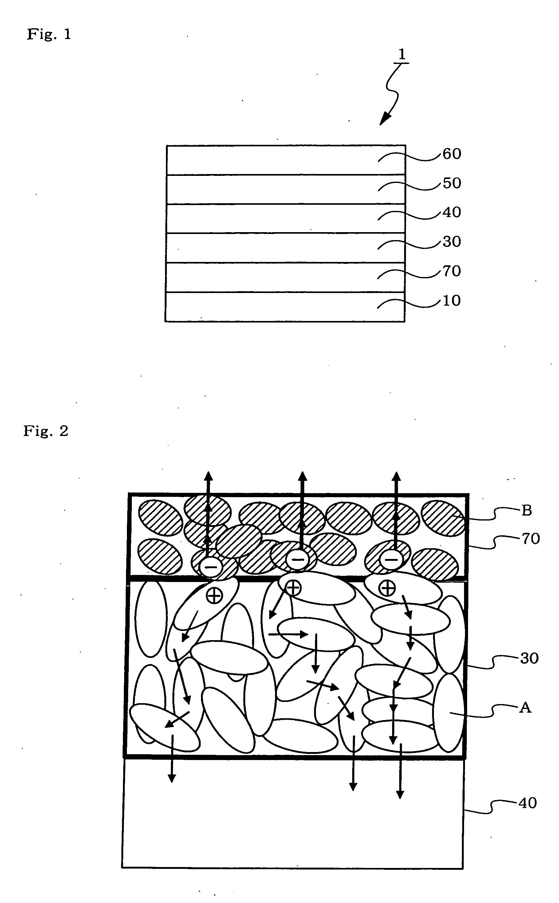
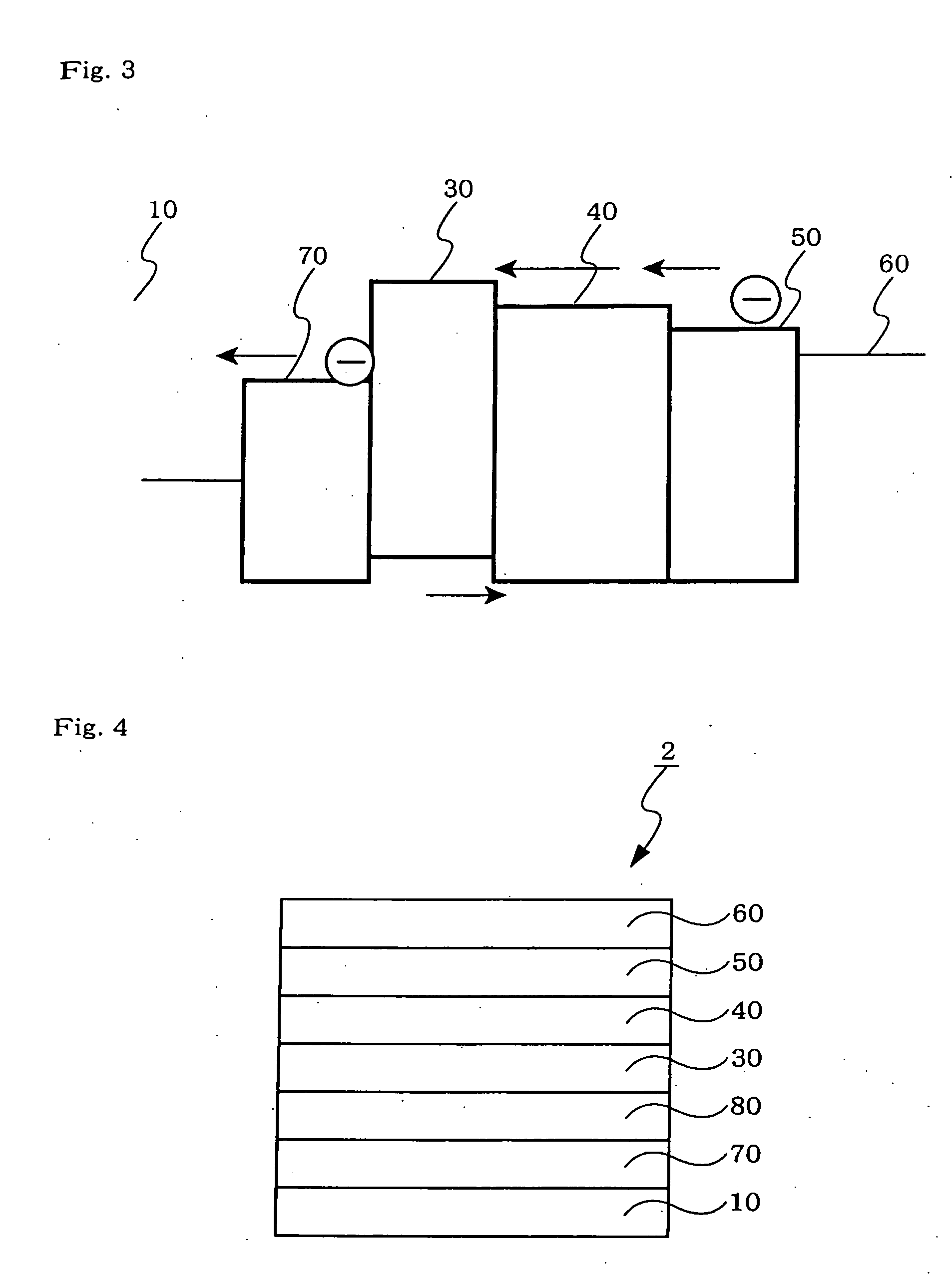
Organic electroluminescent device
a technology of electroluminescent devices and electroluminescent layers, which is applied in the direction of luminescent compositions discharge tubes/lamp details, etc., can solve the problems of deterioration of arylamine compounds, low electron transport capacity of arylamine compounds, and difficulty in measuring the ease of compound reduction, etc., to achieve easy reduction and reduction. the effect of easy measurement and reduction
- Summary
- Abstract
- Description
- Claims
- Application Information
AI Technical Summary
Benefits of technology
Problems solved by technology
Method used
Image

Examples
example 1
[0121] A compound A described below was selected as a material for forming an acceptor-containing layer. In a cyclic voltammetric measurement thereof wherein a saturated calomel electrode (SCE) was used as a reference electrode, the reduction potential thereof was 0.71 V.
[0122] Al as an electrode material and the compound A as a material for forming an acceptor-containing layer were each mounted on a molybdenum heating boat of a vacuum deposition device. A 150 nm thickness Al layer, a 200 nm thickness layer made of the compound A, and a 150 nm thickness Al layer were formed on a 0.7 mm thickness glass substrate in this order.
[0123] A voltage of 1 V was applied across the resultant two Al electrodes, and the value of the current flowing therein was measured. The value was 251 mA / cm2.
(Fabrication of Organic EL Device)
[0124] An ITO film was formed on a 0.7 mm thick glass substrate by using a sputtering method to a thickness of 130 nm. The substrate was subjected to ultrasonic cle...
example 2
[0128] An organic EL device was fabricated in the same manner as in Example 1 except that after forming the acceptor-containing layer, a P-doped layer was formed to a thickness of 50 nm at a ratio of the second hole-transporting material HT2 to compound A of 100:5, and the HT1 film as the first hole-transporting layer was then formed to a thickness of 20 nm.
example 3
[0129] An organic EL device was fabricated in the same manner as in Example 1 except that after forming the acceptor-containing layer, a molybdenum oxide MoO3 film was formed to a thickness of 5 nm.
PUM
 Abstract
Description
Claims
Application Information