Method for fabricating semiconductor device with metal-polycide gate and recessed channel

a metal-polycide gate and recessed channel technology, applied in the direction of semiconductor devices, basic electric elements, electrical appliances, etc., can solve the problems of increasing the electrical thickness of the gate oxide layer b>, poor characteristics, and limitations in the realization of gate resistance and threshold voltage, etc., to achieve the effect of increasing the word line resistan

Inactive Publication Date: 2007-05-24
SK HYNIX INC
View PDF5 Cites 8 Cited by
  • Summary
  • Abstract
  • Description
  • Claims
  • Application Information

AI Technical Summary

Problems solved by technology

Accordingly, planar transistor structures suffer from limitations in the realization of their gate resistance and threshold voltage.
However, the content of fluorine (F) components within the amorphous tungsten silicide (WSix) layer is increased due to the use of the excess WF6 gas, which increases the electrical thickness of the gate oxide layer 150 and causes poor characteristics (e.g., gate oxide integrity (GOI)).
Therefore, the method causes many problems in practical applications.

Method used


Image

  • Method for fabricating semiconductor device with metal-polycide gate and recessed channel
  • Method for fabricating semiconductor device with metal-polycide gate and recessed channel
  • Method for fabricating semiconductor device with metal-polycide gate and recessed channel

Examples


Embodiment Construction

[0033] Preferred embodiments of the invention will be described in detail with reference to the accompanying drawings. However, various variations and modifications can be made in the embodiments and the invention is not to be construed as limited to the following embodiments.

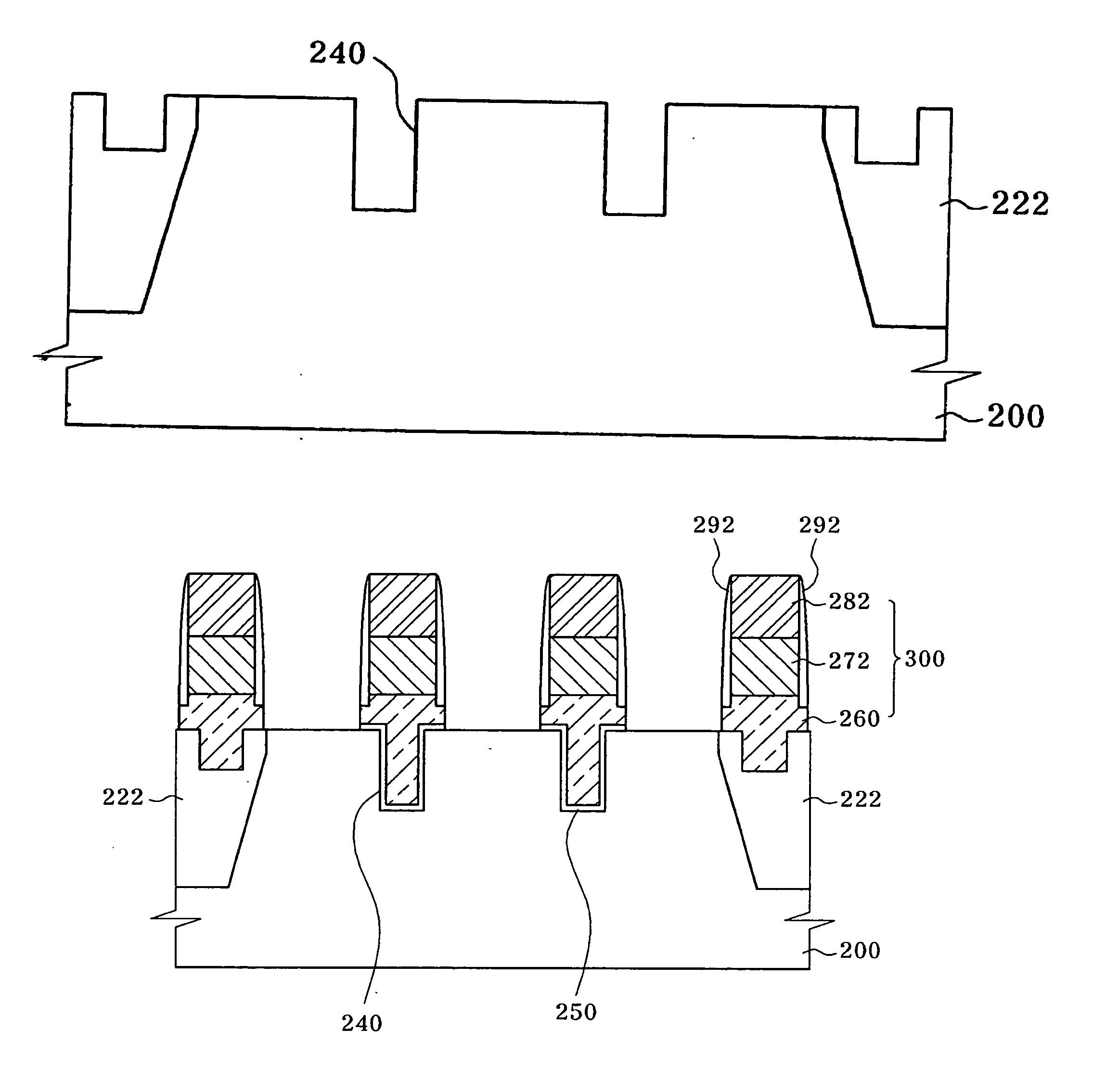
[0034] FIGS. 9 to 17 are cross-sectional views illustrating a method for fabricating a semiconductor device with a tungsten-polycide gate and a recessed channel according to the invention.

[0035] With reference first to FIG. 9, a pad oxide layer 211′ and a pad nitride layer 212′ are sequentially formed on a semiconductor substrate 200 to form a hard mask 210′ for the formation of trenches for isolation. The pad oxide layer 211′ is illustratively formed to have a thickness of about 50 Å to about 150 Å, and the pad nitride layer 212′ is illustratively formed to have a thickness of about 500 Å to about 1,000 Å.

[0036] Referring to FIG. 10, portions of the surface of the semiconductor substrate 200, particularly i...


PUM


Abstract

A method for fabricating a semiconductor device with a metal-polycide gate and a recessed channel, including the steps of: forming trenches for a recessed channel in an active area of a semiconductor substrate; forming a gate insulating layer on the semiconductor substrate having the trenches; forming a gate conductive layer on the entire surface of the resulting structure so that the trenches are buried; forming a silicon-rich amorphous metal silicide layer and a gate hard mask on the gate conductive layer; etching the resulting structure until upper portions of the gate conductive layer are removed by a predetermined thickness, upon first patterning for gate stacks, and forming a metal layer on the entire surface of the resulting structure; forming lateral metal capping layers on sides of the silicon-rich amorphous metal silicide layer by blanket etching, completing formation of gate stacks; and thermally processing the silicon-rich amorphous metal silicide layer to form a crystallized metal silicide layer.

Description

BACKGROUND OF THE INVENTION [0001] 1. Field of the Invention [0002] The invention relates generally to a method for fabricating a semiconductor device and, more particularly, to a method for fabricating a semiconductor device with a metal-polycide gate and a recessed channel. [0003] 2. Description of the Related Art [0004] With drastic decreases in the design rule of integrated circuit semiconductor devices to a level of 70 nm or less, the gate resistance of cell transistors has greatly increased and the channel length of cell transistors has markedly decreased. Accordingly, planar transistor structures suffer from limitations in the realization of their gate resistance and threshold voltage. Under such circumstances, a great deal of research has been recently conducted on methods for ensuring a longer channel length without any increase in design rule. Particularly, studies are actively being undertaken on structures that have an extended channel length while maintaining a limited ...

Claims


Application Information

Patent Timeline
Patent Type & Authority Applications(United States)
IPC IPC(8): H01L21/8234H01L21/336
CPCH01L21/823412H01L21/823437H01L29/4236H01L29/42376H01L29/66621H01L21/18
Inventor KIM, TAE KYUN
Owner SK HYNIX INC
Why Eureka
Try Eureka