

Organic electroluminescent device
a technology of electroluminescent devices and electroluminescent tubes, which is applied in the direction of discharge tubes/lamp details, luminescent compositions, discharge tubes/lamp details, etc., can solve the problems of insufficient luminous efficiency of the emitting device, complex device structure, and remarkable shortening of life, etc., to achieve excellent color purity and long life
- Summary
- Abstract
- Description
- Claims
- Application Information
AI Technical Summary
Benefits of technology
Problems solved by technology
Method used
Image

Examples
example 1
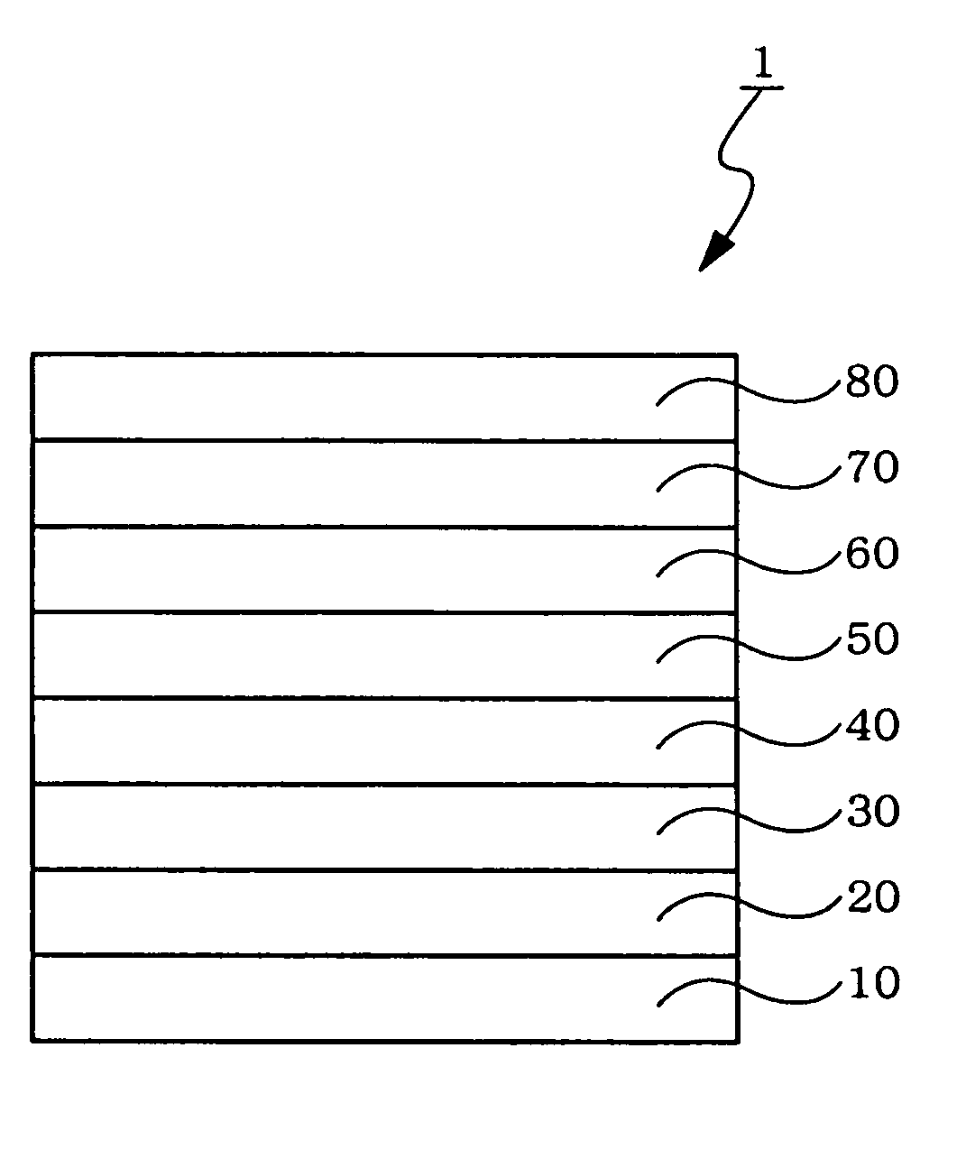
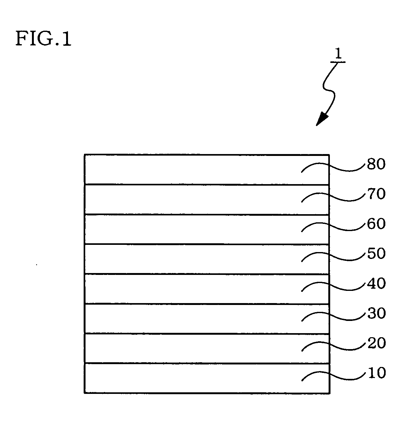
[0102] A transparent electrode made of an indium tin oxide with a thickness of 120 nm was provided on a grass substrate measuring 25 mm by 75 mm by 0.7 mm. The grass substrate was subjected to ultrasonic cleaning with isopropyl alcohol for 5 minutes, and cleaned with ultraviolet ozone for 30 minutes. The resultant substrate was mounted in a vacuum deposition device.
[0103] N′,N″-bis[4-(diphenylamino)phenyl]-N′,N″-diphenylbiphenyl-4,4′-diamine was deposited to form a 60 nm thick film as an hole-injecting layer on the substrate. Thereafter N,N′-bis[4′-{N-(naphthyl-1-yl)-N-phenyl}aminobiphenyl-4-yl]-N-phenylamine was deposited to form a 10 nm thick film as a hole-transporting layer thereon.
[0104] The ionization potential of the hole-transporting layer was 5.5 eV.
[0105] The ionization potential was measured by a cyclic voltammetry or a photoerectoron spectroscopy. The host material of the emitting layer was measured in the same way.
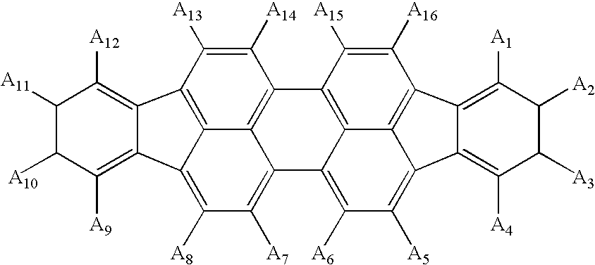
[0106] Next, the compound (A-1) of a naphthacene der...
example 2
[0113] An organic EL device was fabricated in the same way as in Example 1 except that the compound (C-2) was used instead of the compound (C-1) when the electron-transporting layer was formed.
[0114] For the organic EL device thus obtained, a conduction test was performed. Red emission with a driving voltage of 4.5 V and emission luminance of 716 cd / m2 was obtained at a current density of 10 mA / cm2. The chromaticity was (0.65, 0.33) and the efficiency was 7.16 cd / A. At this time, the peak intensity derived from a material other than the dopant was 1 / 59 of that derived from the dopant. A direct current continuous applying test was conducted at an initial luminance of 5000 cd / m2, and a period of time until the luminance reached 80% of the initial luminance was 1190 hours.
example 3
[0117] An organic EL device was fabricated in the same way as in Example 1 except that the compound (A-3) below of a diaminoanthracene derivative was used instead of the compound (A-1) when the emitting layer was formed.
Ionization potential: 5.5 eV
[0118] For the organic EL device thus obtained, a conduction test was performed. Red emission with a driving voltage of 4.1 V and emission luminance of 978 cd / m2 was obtained at a current density of 10 mA / cm2. The chromaticity was (0.67, 0.33) and the efficiency was 9.78 cd / A. At this time, the peak intensity derived from a material other than the dopant was 1 / 184 of that derived from the dopant. A direct current continuous applying test was conducted at an initial luminance of 5000 cd / m2, and a period of time until the luminance reached 80% of the initial luminance was 1544 hours.
PUM
 Abstract
Description
Claims
Application Information