

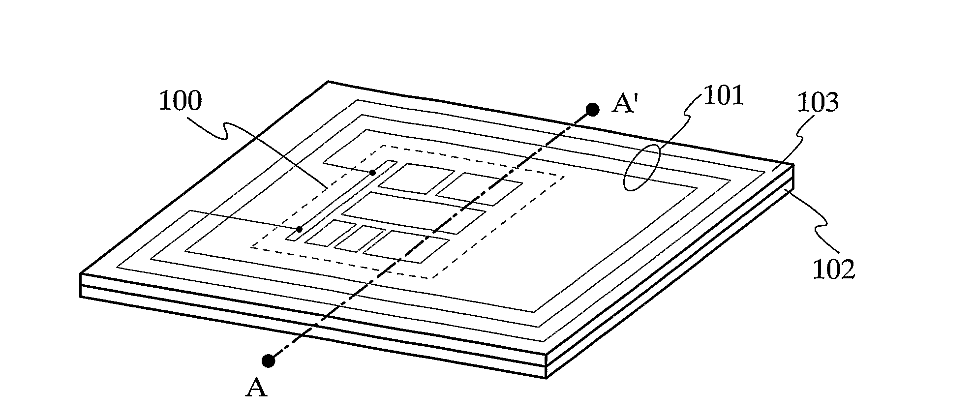
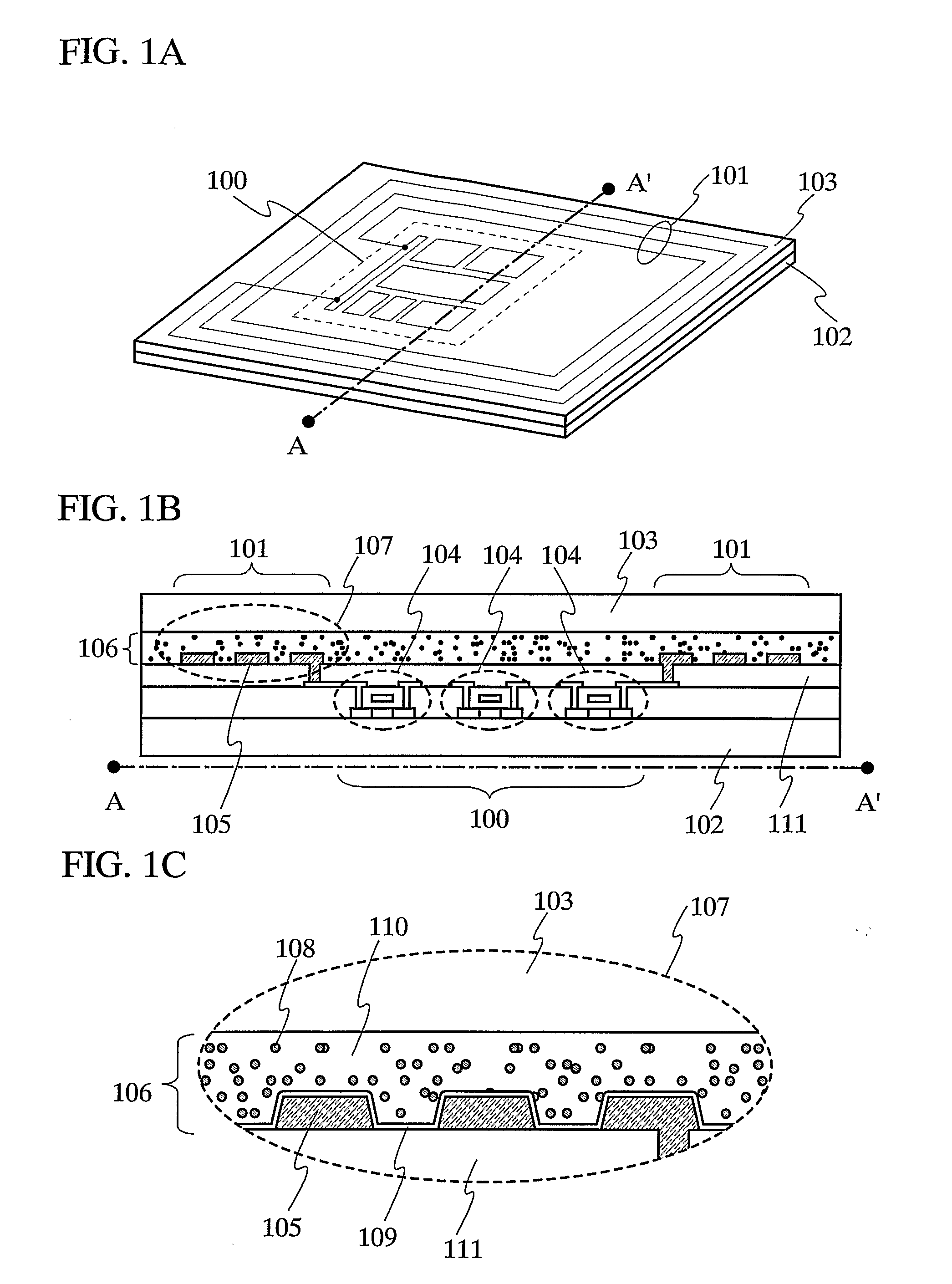
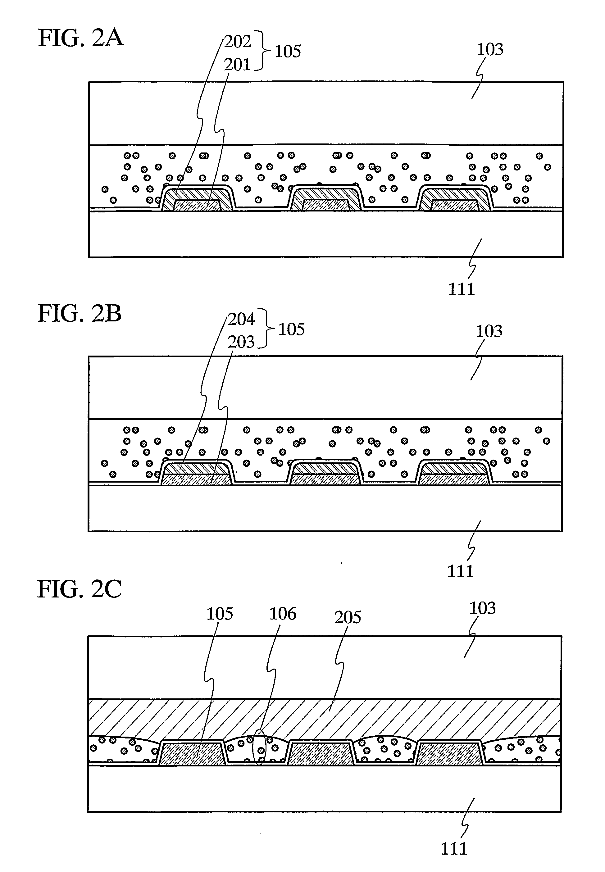
Semiconductor device
a technology of electromagnetic field and semiconductor device, which is applied in the direction of burglar alarm mechanical actuation, burglar alarm by hand-portable object removal, instruments, etc., can solve the problems of difficult to increase the process yield, low reliability, and inability to detect in a connection portion easily caused, so as to achieve small coercivity, increase mutual inductance of antennas, and high permeability
- Summary
- Abstract
- Description
- Claims
- Application Information
AI Technical Summary
Benefits of technology
Problems solved by technology
Method used
Image

Examples
embodiment 2
[0146] Embodiment 2 describes one mode of a functional configuration of a semiconductor device such as an ID chip according to the present invention with reference to FIG. 11.
[0147] In FIG. 11, reference numeral 900 denotes an antenna, 901 denotes an integrated circuit, and 903 denotes a capacitor formed between both terminals of the antenna 900. The integrated circuit 901 includes a demodulation circuit 909, a modulation circuit 904, a rectification circuit 905, a microprocessor 906, a memory 907, and a switch 908 for providing load modulation to the antenna 900. In addition, the number of the memory 907 is not limited to one; a plurality of the memories 907 may be provided. As the memory 907, a SRAM, a flash memory, a ROM, a FRAM (registered mark), or the like may be used.
[0148] A signal sent from the reader / writer as a radio wave is converted into an alternating electric signal by electromagnetic induction in the antenna 900. The alternating electric signal is demodulated in th...
embodiment 3
[0152] Embodiment 3 describes a structure of a TFT used in a semiconductor device such as an ID chip of the present invention.
[0153]FIG. 12A shows a cross sectional view of TFT according to the embodiment. Reference numeral 701 represents an n-channel TFT; and 702, a p-channel TFT. The configuration of the n-channel TFT 701 will be explained in detail as an example.
[0154] The n-channel TFT 701 includes an island-like semiconductor film 705 to be used as an active layer. The island-like semiconductor film 705 includes two impurity regions 703 to be used as a source region and a drain region, a channel formation region 704 sandwiched between the two impurity regions 703, and two LDD (lightly doped drain) regions 710 sandwiched between the impurity regions 703 and the channel formation region 704. The n-channel TFT 701 further includes a gate insulating film 706 covering the island-like semiconductor film 705, a gate electrode 707, and two sidewalls 708 and 709 made from insulating f...
embodiment 4
[0167] In this embodiment, a method for manufacturing plural semiconductor devices such as ID chips with the use of a large size substrate will be described.
[0168] An integrated circuit 401 and an antenna 402 are formed over a heat resistant substrate. Thereafter, the integrated circuit 401 and the antenna 402 are both separated from the heat resistant substrate and attached to a substrate 403, which has been separately prepared, with an adhesive agent 404 as shown in FIG. 13A. Although FIG. 13A shows a mode in which a set of the integrated circuit 401 and the antenna 402 is attached to the substrate 403, the present invention is not limited to this configuration. Alternatively, a plurality of sets of the integrated circuit 401 and the antenna 402, which are connected to each other, may be separated from the heat resistant substrate and attached onto the substrate 403 at the same time.
[0169] As shown in FIG. 13B, a cover material 405 is attached to the substrate 403 such that the ...
PUM
 Abstract
Description
Claims
Application Information