Built-in capacitor type wiring board and method for manufacturing the same

a technology of built-in capacitors and wiring boards, which is applied in the direction of fixed capacitors, stacked capacitors, fixed capacitor details, etc., can solve the problems of deterioration in the reliability of the wiring boards, the tendency of the capacitor to misalign in the planar direction, etc., and achieves the effect of preventing the delamination of the outer circumference portion of the capacitor, facilitating the production of capacitors, and reducing the strength degradation of the capacitor due to the formation

Inactive Publication Date: 2007-05-31
NGK SPARK PLUG CO LTD
View PDF11 Cites 69 Cited by
  • Summary
  • Abstract
  • Description
  • Claims
  • Application Information

AI Technical Summary

Benefits of technology

[0025] Although the hole portion may be a non-through-hole opening only at the second main surface or may be a through-hole opening at both first main surface and the second main surface, a through-hole is preferable. In this way, the hole portion can be formed by a simple boring process, thereby easily producing the capacitor. Since a part of the interlayer insulating layer flows into the hole portion when disposing the capacitor on the interlayer insulating layer, misalignment of the capacitor in the planar direction can be prevented. Further, while a part of the interlayer insulating layer flows into the hole portion, only a small quantity of the interlayer insulating layer is pushed out from the end face of the second surface of the capacitor. Thus, the coplanar relation of the interlayer insulating layer is secured. Furthermore, since a part of the interlayer insulating layer flowing into the hole portion extends to the interlayer insulating layer on the first main surface of the capacitor, the capacitor is more tightly fixed in the multilayer portion (i.e., between the interlayer insulating layers).
[0026] Although the hole portion may be disposed in any part of the capacitor, the hole portion is preferably disposed in plural locations along the outer circumference of the capacitor. In this way, the interlayer insulating layer is unlikely to be pushed out fr

Problems solved by technology

A significant disadvantage of the above-described approach, wherein the capacitor is embedded in a built-up layer, is that the capacitor tends to misalign in the planar direction when being mounted on an insulating lay

Method used


Image

  • Built-in capacitor type wiring board and method for manufacturing the same
  • Built-in capacitor type wiring board and method for manufacturing the same
  • Built-in capacitor type wiring board and method for manufacturing the same

Examples


first embodiment

[0057] Hereinafter, a first embodiment of a built-in capacitor type wiring board in accordance with the present invention will be described in detail with reference to the drawings.

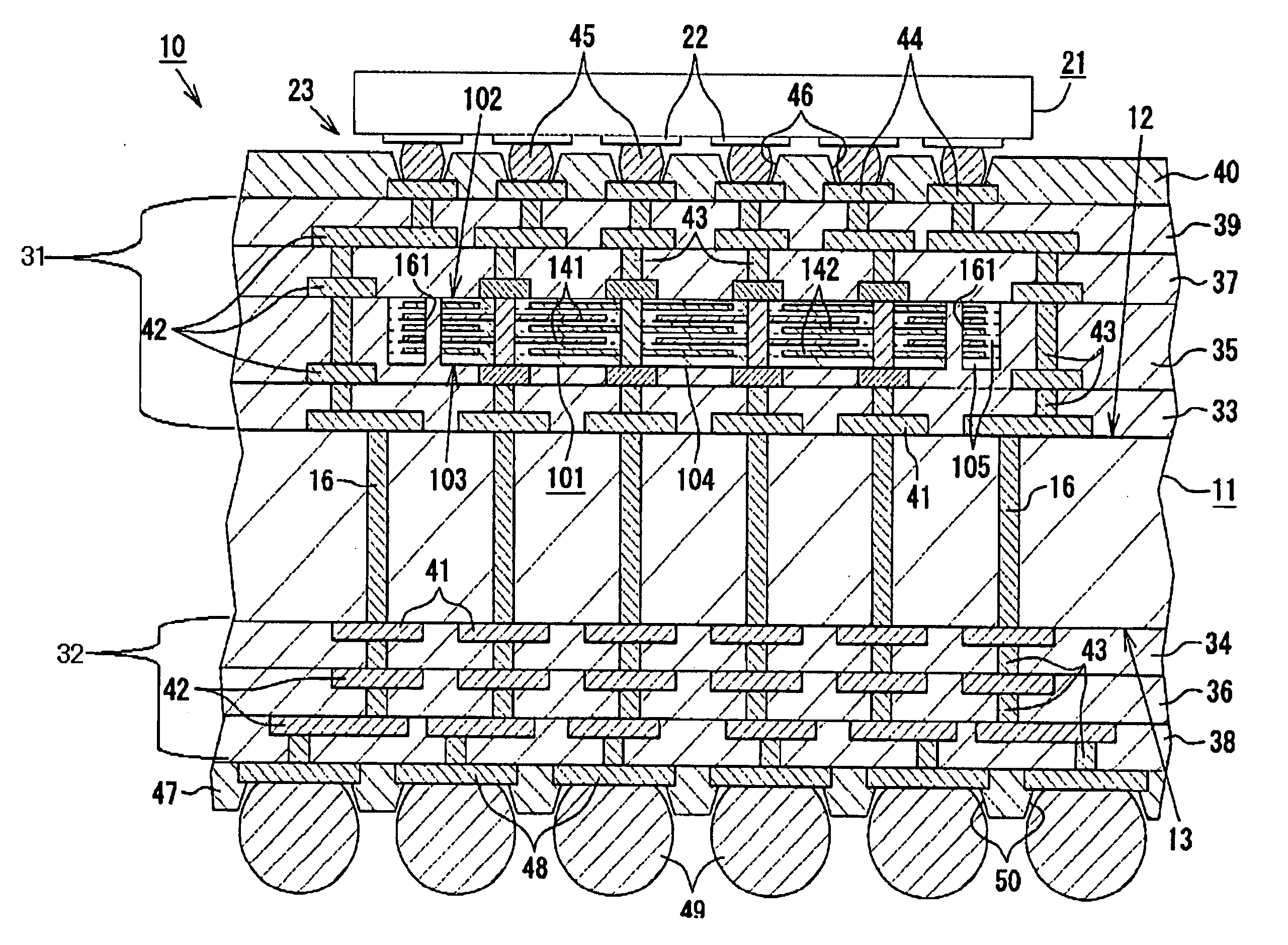
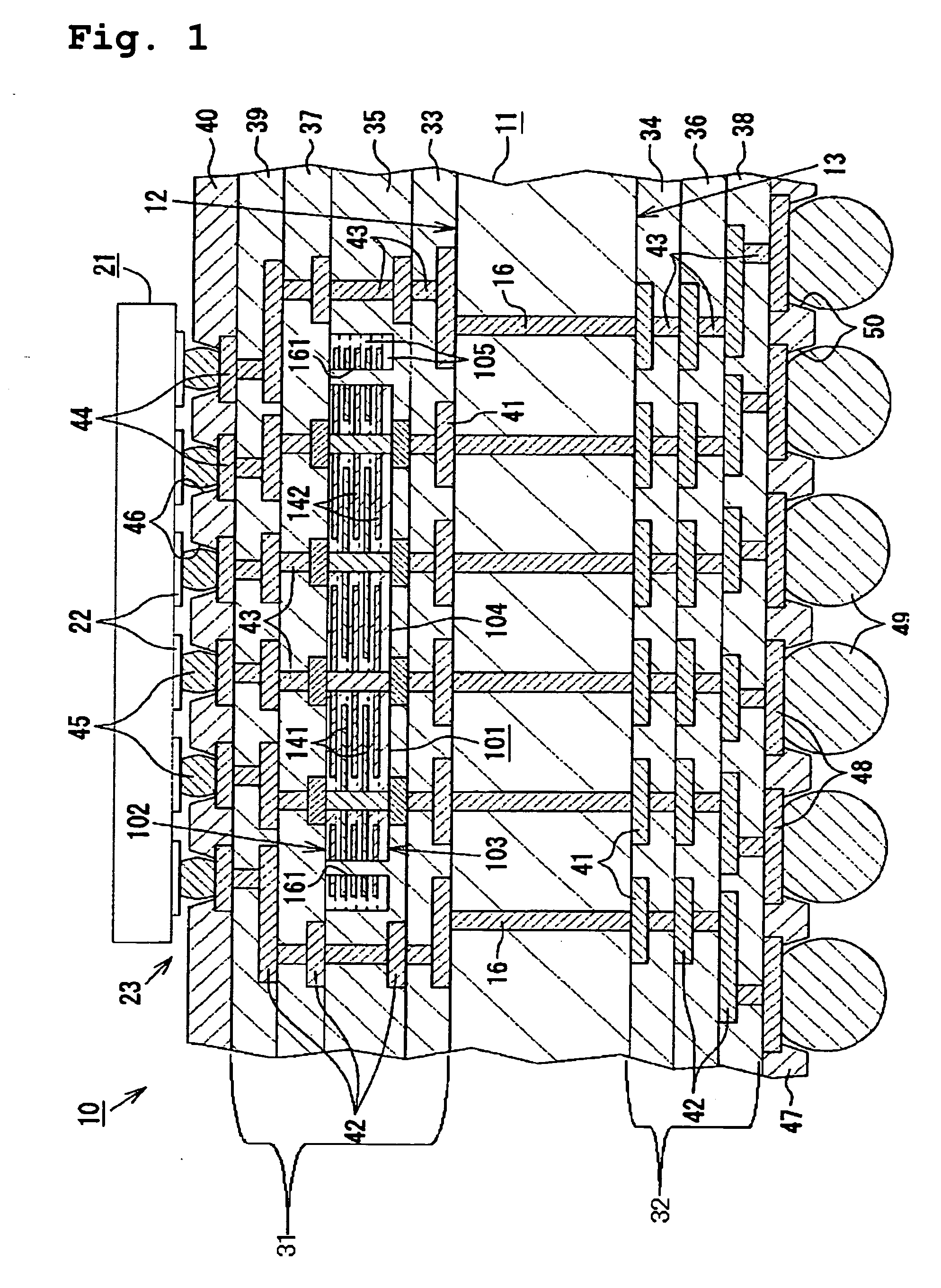
[0058] As shown in FIG. 1, a built-in capacitor type wiring board 10 according to this embodiment is a wiring board for mounting an IC chip, and comprises: a substrate core 11 comprised of glass epoxy and of a generally rectangular shape; a built-up layer 31 (a multilayer portion) formed on an upper surface 12 of the substrate core 11; and a built-up layer 32 formed on an lower surface 13 of the substrate core 11. Via conductors 16 are formed at plural locations in the substrate core 11. The via conductors 16 electrically connect the upper surface 12 and the lower surface 13 of the substrate core 11. Conductor layers 41, comprised of copper, are formed in a pattern on both upper surface 12 and lower surface 13 of the substrate core 11 so that each conductor layer 41 is electrically connected to the via c...

second embodiment

[0087] A built-in capacitor type wiring board 201 of a second embodiment will now be described in detail with reference to FIGS. 13 to 15. In this description, only the parts or portions of the built-in capacitor type wiring board 201 that are different from that of the first embodiment will be described. The same reference numerals are used for components constructed in the same manner as the built-in capacitor type wiring board 101, and any detailed description thereof will be omitted.

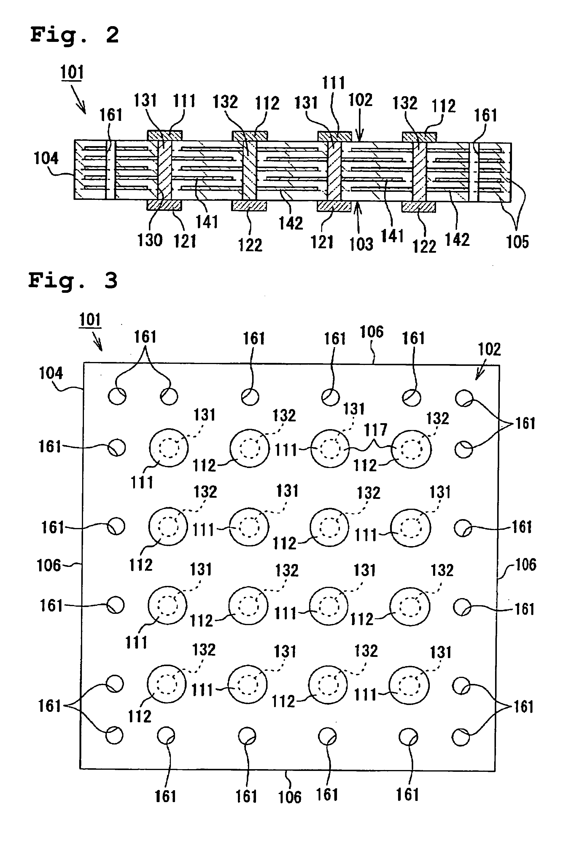
[0088] As shown in FIG. 13, in the built-in capacitor type wiring board 201, the built-up layer 31 has a structure wherein resin insulating layers 202, 203, 204, 205, 206, 207 (the so-called interlayer insulating layers) and a conductor layer 42 are alternately laminated, which is different from the structure of the first embodiment. Further, as shown in FIGS. 13 to 15, a built-in capacitor for a wiring board 211 (hereinafter referred to as “capacitor 211”) embedded in the built-in capacitor type wi...


PUM


Abstract

In order to provide a built-in capacitor type wiring board capable of preventing misalignment of the capacitor, a capacitor built-in type wiring board is provided which includes a core board; a multilayer portion disposed on at least one side of the core board and formed by a plurality of interlayer insulating layers; and a plurality of conductor layers alternately laminated on the core board. The capacitor is of a chip-like shape with first and second main surfaces and includes a dielectric layer; electrode layers laminated on the dielectric layer; and a hole portion opening at least at the second main surface. The capacitor is embedded in the interlayer insulating layers so that the second main surface faces the core board.

Description

FIELD OF THE INVENTION [0001] The present invention relates to a built-in capacitor type wiring board including a built-in capacitor for a wiring board, and to a method for manufacturing the same. BACKGROUND OF THE INVENTION [0002] In recent years, semiconductor integrated circuit elements (IC chips) used for a CPU in computers or the like operate at higher speeds with more high level functional features than previously. Along with this advance, the number of terminals has increased and the terminal interval has tended to be smaller or narrower. Generally speaking, in such a construction, terminals in large numbers are densely formed on the bottom surface of the IC chip in an array, and a terminal block so formed is connected to a further terminal block at the motherboard side by a conventional “flip chip” connection. However, because there is a large difference in pitch between the terminal block at the IC chip side and the terminal block at the motherboard side, it is difficult to...

Claims


Application Information

Patent Timeline
IPC IPC(8): H01G4/228
CPCH01G4/232H01L2224/16235H01L23/49822H01L23/49838H01L2224/16237H01L2924/01078H01L2924/09701H01L2924/15174H01L2924/15311H05K1/0231H05K1/112H05K1/185H05K1/186H05K3/4602H05K2201/10674H05K2201/10712H01L2924/01019H01G4/30H01L2224/05573H01L2224/05568H01L2924/00014H01L2224/16225H01L2224/05599
Inventor YAMAMOTO, HIROSHISEKI, TOSHITAKEINUI, YASUHIKOOTSUKA, JUNSATO, MANABU
Owner NGK SPARK PLUG CO LTD
Why Eureka
Try Eureka