Semiconductor device manufacturing method and substrate processing system

a technology of semiconductor devices and processing systems, applied in photomechanical treatment, instruments, electrical equipment, etc., can solve the problems of increasing the dielectric constant, damage, and deteriorating some effects, and achieve excellent electrical characteristics and reliability

Inactive Publication Date: 2007-05-31
TOKYO ELECTRON LTD
View PDF11 Cites 12 Cited by
  • Summary
  • Abstract
  • Description
  • Claims
  • Application Information

AI Technical Summary

Benefits of technology

[0010] An object of the present invention is to provide a semiconductor device manufacturing method to manufacture a semiconductor device

Problems solved by technology

However, according to the conventional damascene process described above, when a resist film is peeled, the inter-level insulating film 501 made of a Low-k material is damaged.
This damage increases the dielectric constant of the inter-level

Method used


Image

  • Semiconductor device manufacturing method and substrate processing system
  • Semiconductor device manufacturing method and substrate processing system
  • Semiconductor device manufacturing method and substrate processing system

Examples


first embodiment

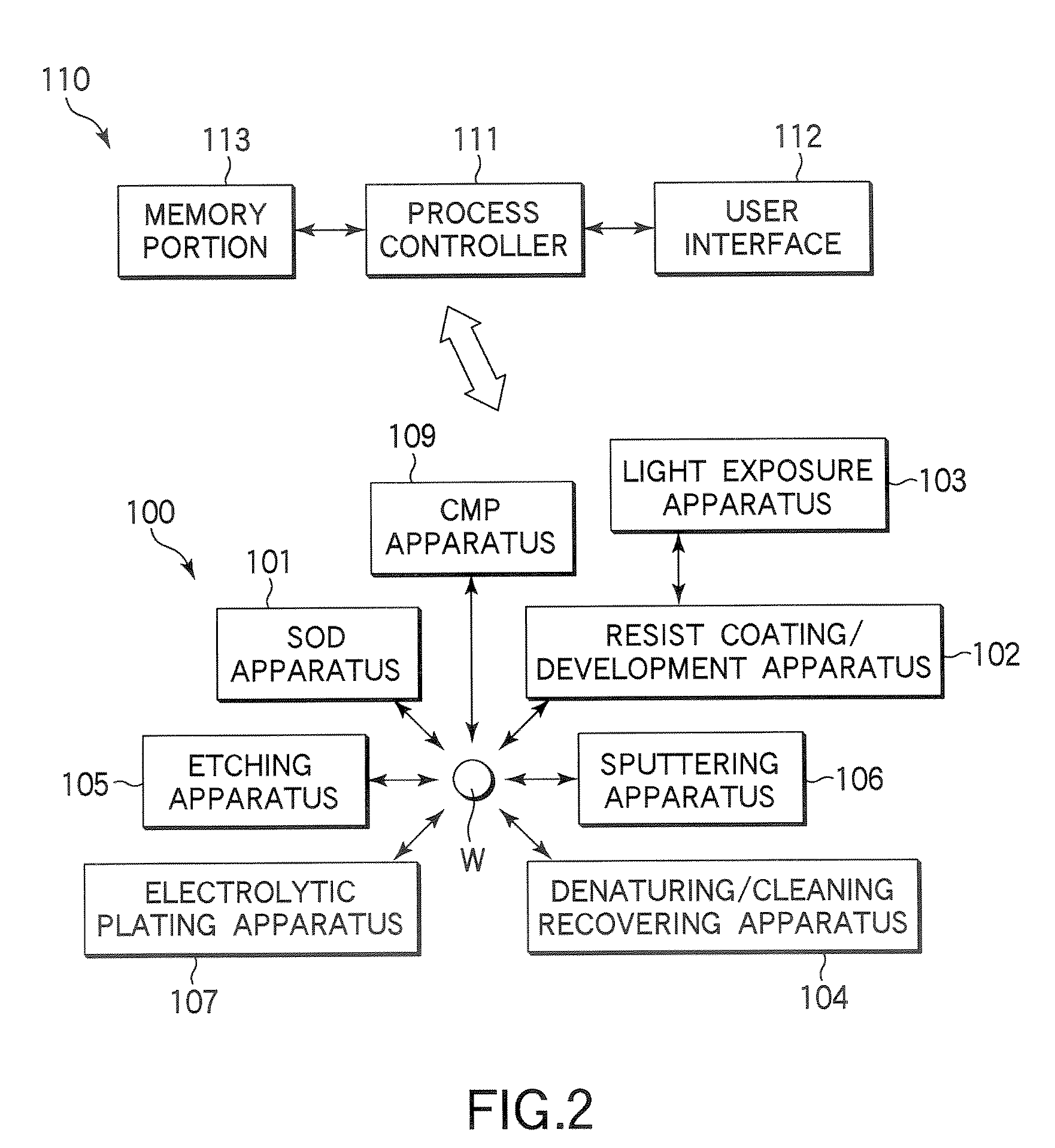
[0060]FIG. 2 is an explanatory view schematically showing the arrangement of a semiconductor device manufacturing system used for a semiconductor device manufacturing process according to the present invention. This semiconductor device manufacturing system includes a process section 100 and a main control section 110. The process section 100 includes an SOD (Spin On Dielectric) apparatus 101, a resist coating / development apparatus 102, a light exposure apparatus 103, a denaturing / cleaning / recovering apparatus 104 for performing resist denaturing, cleaning, and recovery processes, an etching apparatus 105, a sputtering apparatus 106 used as a PVD apparatus, an electrolytic plating apparatus 107, and a CMP apparatus 109 used as a polishing apparatus. The main control section 110 includes a process controller 111, a user interface 112, and a memory portion 113. The SOD apparatus 101, sputtering apparatus 106, and electrolytic plating apparatus 107 of the process section 100 are film f...

second embodiment

[0148] Next, an explanation will be given of a

[0149]FIG. 15 is an explanatory view schematically showing the arrangement of a semiconductor device manufacturing system used for a semiconductor device manufacturing process according to a second embodiment of the present invention. In FIG. 15, the same constituent elements as those described above are denoted by the same reference numerals used in FIG. 2. This semiconductor device manufacturing system includes a process section 100′ and a main control section 110 having the same structure as that shown in FIG. 2. The process section 100′ includes an SOD (Spin On Dielectric) apparatus 101, a resist coating / development apparatus 102, a light exposure apparatus 103, a sputtering apparatus 106, an electrolytic plating apparatus 107, and a CMP apparatus 109 used as a polishing apparatus, which are the same as those in the first embodiment. The process section 100′ further includes an etching / ashing / recovering apparatus 108 for performing d...


PUM


Abstract

A semiconductor device manufacturing method includes: forming an etching mask having a predetermined circuit pattern on a surface of an etching target film disposed on a semiconductor substrate; etching the etching target film through the etching mask to form a groove or hole in the etching target film; removing the etching mask by a process including at least a process using an ozone-containing gas; and recovering damage of the etching target film caused before or in said removing the etching mask, while supplying a predetermined recovery gas.

Description

BACKGROUND OF THE INVENTION [0001] 1. Field of the Invention [0002] The present invention relates to a method of manufacturing a semiconductor device by use of, e.g., a single damascene method or dual damascene method, and a substrate processing system used for manufacturing a semiconductor device. [0003] 2. Description of the Related Art [0004] In semiconductor device manufacturing processes, a dual damascene method is frequently used for forming interconnection lines embedded in trenches and / or connection holes (for example, see Jpn. Pat. Appln. KOKAI Publication No. 2002-83869). FIGS. 1A to 1I are explanatory views schematically showing a method of forming a Cu interconnection line, using a conventional dual damascene method. [0005] At first, for example, an interconnection layer 500, an inter-level insulating film 501, and an anti-reflective coating 502 are formed in this order on a substrate. Further, a first resist film 503 is formed on the surface of the multi-layer structure...

Claims


Application Information

Patent Timeline
IPC IPC(8): G03F7/26
CPCH01L21/3105H01L21/31138H01L21/67051H01L21/67069H01L21/67109H01L21/67178H01L21/67207H01L21/76808H01L21/76814H01L21/76826H01L21/28
Inventor ASAKO, RYUICHIMAEKAWA, KAORUFUJII, YASUSHI
Owner TOKYO ELECTRON LTD
Why Eureka
Try Eureka