Solid state radiation sensor and manufacturing method of the same

Active Publication Date: 2007-06-07
SHIMADZU CORP
View PDF5 Cites 12 Cited by
  • Summary
  • Abstract
  • Description
  • Claims
  • Application Information

AI Technical Summary

Benefits of technology

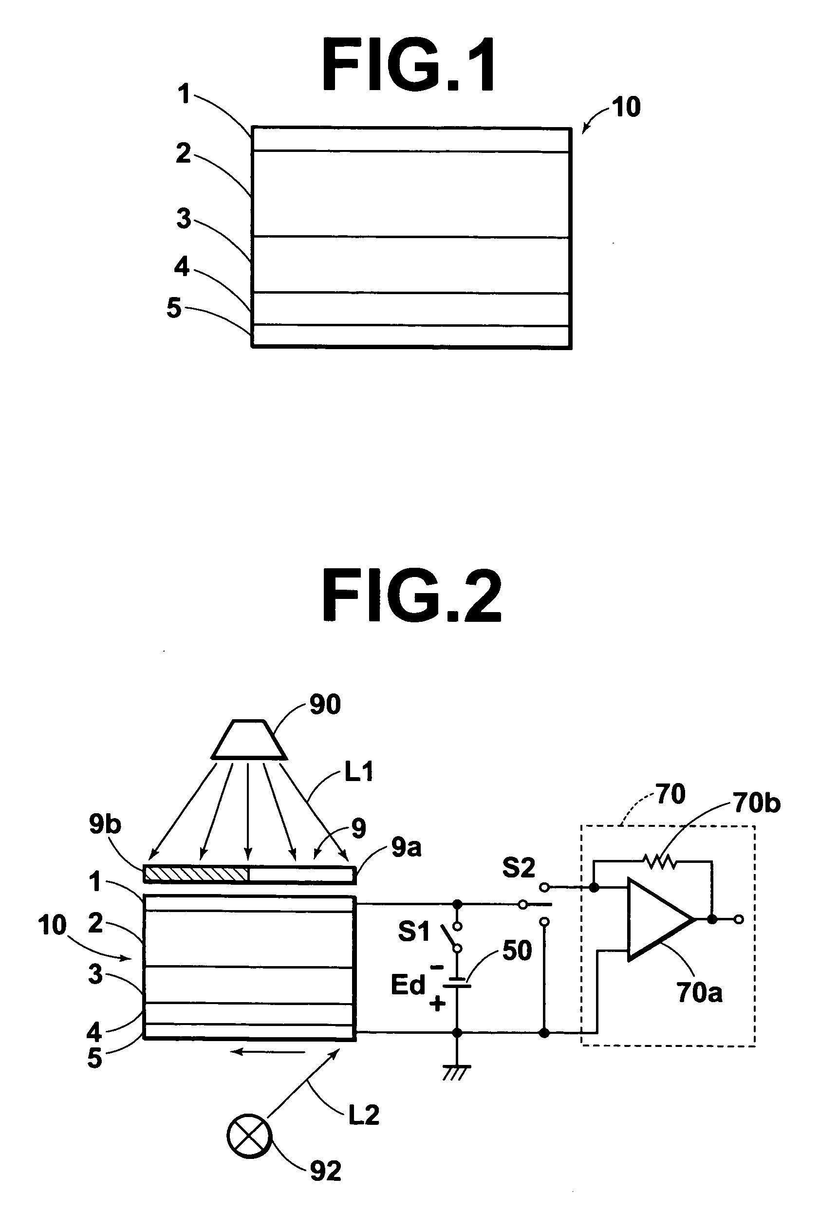
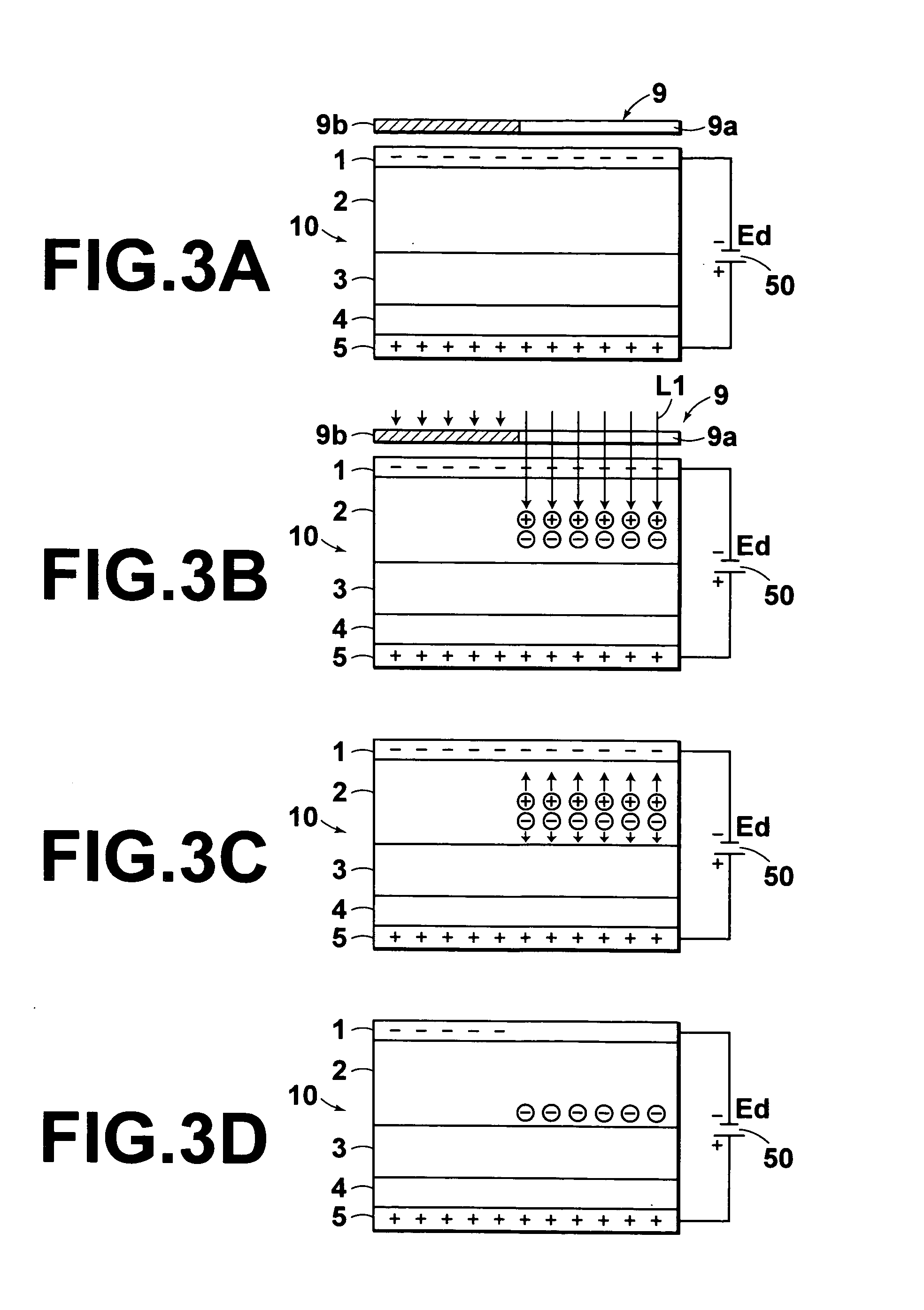
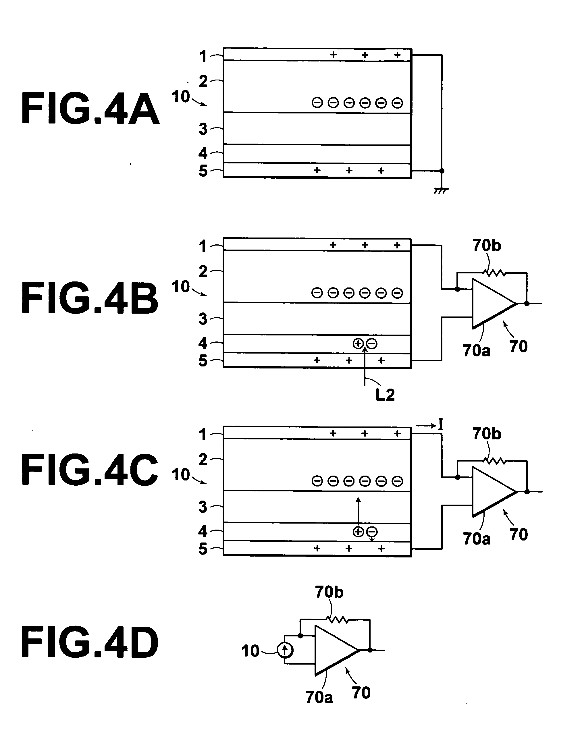
[0018] The first solid state radiation sensor of the present invention is a solid state radiation sensor, in which an electrode is disposed on each side of a recording photoconductive layer, and charges generated in the recording photoconductive layer by the irradiation of radiation, with a predetermined bias voltage being applied between the electrodes, are detected as electrical signals. Here, a predetermined region is provided between the electrodes, and the average density of an alkali metal in the predetermined region is greater than or equal to 10 times the average density thereof in the area between the electrodes other than the predetermined region, so that the first solid state radiation sensor of the present invention has less sensitivity degradation, longer electron lifetime, and superior electron mobility. Further, the solid state radiation sensor of the present invention may not impair the hole mobility characteristics.
[0019] In particular, the solid state radiation sensor of the present invention having the region with a thickness of 5 to 100 nm, and an average alkali metal density of 0.2 to 10 ppm is more preferable, since such solid state radiation sensor may provide both improved electron mobility and minimized cry

Problems solved by technology

The use of amorphous selenium may readily provide large surface area through a thin film forming technique such as vacuum deposition method and the like, but the resultant photoconductive layer have many structural defects because of its amorphous nature, so that the sensitivity of the photoconduc

Method used


Image

  • Solid state radiation sensor and manufacturing method of the same
  • Solid state radiation sensor and manufacturing method of the same
  • Solid state radiation sensor and manufacturing method of the same

Examples


example 11

[0066] After depositing the example 8, the selenium alloy doped with Na of 2 ppm remaining in the evaporation crucible is removed at the temperature of 380 degrees Celsius for 30 minutes. Then, 5N selenium is filled in the same crucible and the device of example 11 was produced in the same manner.

(Measurement of Electron Lifetime)

[0067] Electron lifetime measurements were conducted by the time of flight (TOF) method based on the description, by S. O. Kasap, and J. A. Rowlands, in Journal of Materials Science: Materials in Electronics, II, 179 (2000). Hole lifetime measurements were conducted by reversing the bias voltage.

(Measurement of Charge Collection)

[0068] 10mR X-ray was irradiated on the deposited Se films, which are the recording photoconductive layers obtained in the examples 1 to 10 and comparative examples 1 and 2, for 0.2 seconds using a Mo tube with a voltage of 30 kV. A pulsating photocurrent generated in the Se films with a voltage being applied thereto was conve...


PUM


Abstract

A solid state radiation sensor, in which an electrode is disposed on each side of a recording photoconductive layer, and charges generated in the recording photoconductive layer by the irradiation of radiation, with a predetermined bias voltage being applied between the electrodes, are detected as electrical signals. Here, a predetermined region is provided between the electrodes, and the average density of an alkali metal in the predetermined region is greater than or equal to 10 times the average density of the alkali metal in the area between the electrodes other than the predetermined region.

Description

BACKGROUND OF THE INVENTION [0001] 1. Field of the Invention [0002] The present invention relates to a solid state radiation sensor, suitable for use with an imaging apparatus using radiation, such as X-rays or the like, and a manufacturing method of the sensor. [0003] 2. Description of the Related Art [0004] In the field of medical X-ray imaging, X-ray imaging panels (solid state radiation sensors) are known. The X-ray imaging panel uses an X-ray sensitive photoconductive layer as a photoconductor, in order to improve diagnostic capabilities with a reduced amount of radiation received by a subject, and an electrostatic latent image formed by the X-rays on the photoconductive layer is read out by light or multitudes of electrodes and recorded. The method described above is superior to the known image projection method called indirect imaging using TV camera tube, in that it may obtain higher resolution. [0005] The X-ray imaging panel described above includes therein a charge generat...

Claims


Application Information

Patent Timeline
IPC IPC(8): G01T1/24
CPCH01L27/1462H01L27/14632H01L27/14676H01L27/14692H01L27/307H01L31/0272G01T1/246H10K39/32
Inventor MIYAKE, KIYOTERUNABETA, TOSHIYUKITAKAHASHI, KENJIIRISAWA, KAKUIMAI, SHINJI
Owner SHIMADZU CORP
Why Eureka
Try Eureka