Isolation structures for semiconductor integrated circuit substrates and methods of forming the same

a technology of integrated circuit substrate and isolation structure, which is applied in the direction of semiconductor devices, semiconductor/solid-state device details, electrical apparatus, etc., can solve the problems of reducing the value of the isolation structure of the trench, reducing the processing efficiency of the trench, so as to achieve high flexibility

Inactive Publication Date: 2007-06-14
ADVANCED ANALOGIC TECHNOLOGIES INCORPORATED
View PDF9 Cites 99 Cited by
  • Summary
  • Abstract
  • Description
  • Claims
  • Application Information

AI Technical Summary

Benefits of technology

[0017] The methods of this invention are highly flexible and can be used to form isolation regions necessary meet the varying demands of different regions and devices in a semiconductor substrate. The topography of the substrate is maintained extremely flat, or at least sufficiently flat as not to interfere with or complicate the formation of fine line widths and submicron features or the interconnection thereof during subsequent processing. Protective caps can be used to protect the dielectric materials from erosion during subsequent processing.

Problems solved by technology

The problem with forming a dielectric-filled trench early in the process it that subsequent process steps, which frequently include etching and cleaning, can etch or erode the dielectric material in the trench.
This can impair the value of the trench as an isolation structure and can create depressions in the top surface of the chip, rendering further processing more difficult.
Dielectric materials that are resistant to etching in normal semiconductor processes (e.g., silicon nitride) tend to be hard, brittle, high-stress materials.
When these materials are deposited in a trench they tend to crack.
A second problem stems from the fact that chips are generally divided into two general areas: broad or wide “field” areas and more densely-packed device areas, sometimes referred to as “active” areas.
This creates a problem in filling the trenches.
The narrow trenches may be filled while the wide trenches are difficult to fill.
Alternatively, using numerous narrow trenches to cover large distances in the field areas can complicate the topography of the chip.

Method used


Image

  • Isolation structures for semiconductor integrated circuit substrates and methods of forming the same
  • Isolation structures for semiconductor integrated circuit substrates and methods of forming the same
  • Isolation structures for semiconductor integrated circuit substrates and methods of forming the same

Examples


Embodiment Construction

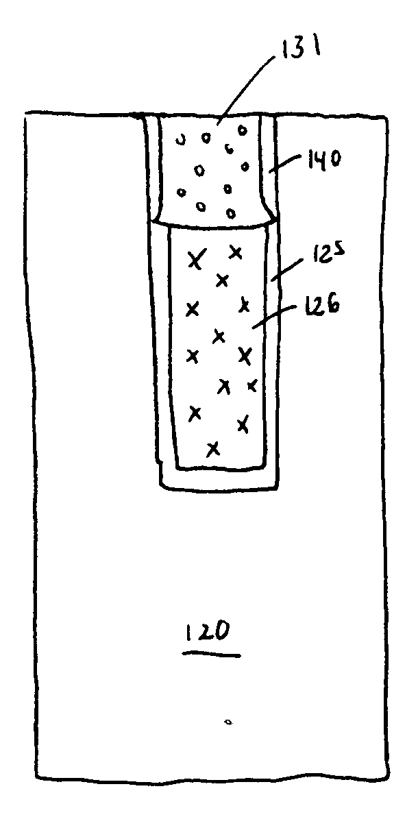
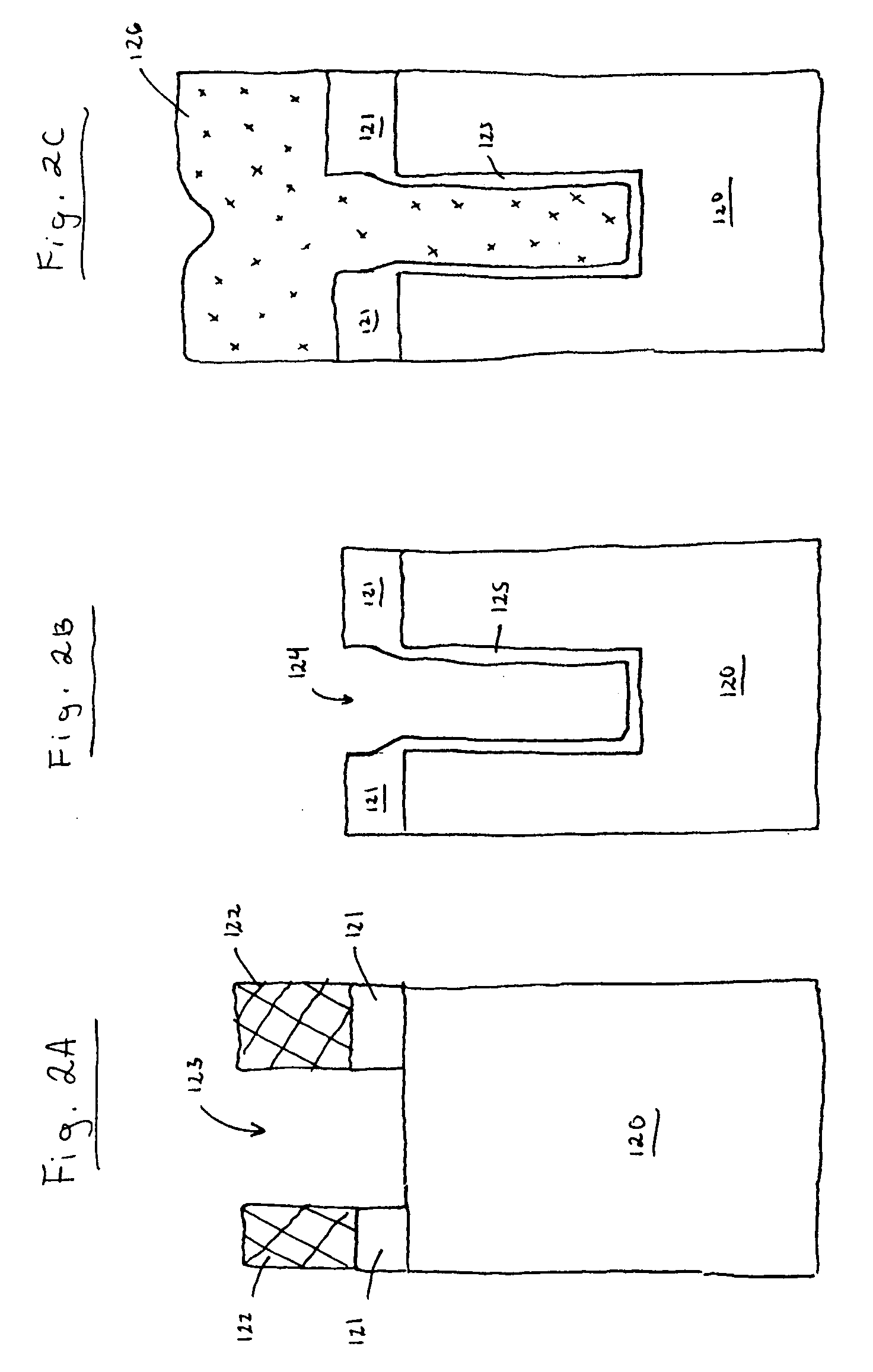
[0027]FIGS. 2A-2F illustrate a process for fabricating a trench isolation structure that avoids the formation of a gap or recess at the top of the trench, as shown in FIG. 1C. As shown in FIG. 2A, an oxide or “hard mask” layer 121 is formed on the top surface of a semiconductor substrate 120, and a photoresist layer 122 is deposited on top of hard mask layer 121. The term “hard mask” is used herein to refer to a thermally grown or deposited dielectric layer used as a mask during the etching of a trench in semiconductor substrate 120. The “hard mask” is distinguished from the organic photoresist layer 122, for example, which is mechanically softer and therefore subject to erosion during the trench etch process. An opening is formed in photoresist layer 122 by a normal photolithographic process, and an opening 123 is etched in hard mask layer 121 through the opening in photoresist layer 122.

[0028] As shown in FIG. 2B, substrate 120 is etched through the opening 123 to form a trench 1...


PUM


Abstract

Isolation regions for semiconductor substrates include dielectric-filled trenches and field oxide regions. Protective caps of dielectric materials dissimilar from the dielectric materials in the main portions of the trenches and field oxide regions may be used to protect the structures from erosion during later process steps. The top surfaces of the isolation structures are coplanar with the surface of the substrate. Field doping regions may be formed beneath the field oxide regions. To meet the demands of different devices, the isolation structures may have varying widths and depths.

Description

FIELD OF THE INVENTION [0001] This invention relates to semiconductor chip fabrication and in particular to methods of fabricating structures to isolate electrically the active or passive devices formed on a semiconductor chip. BACKGROUND OF THE INVENTION [0002] In the fabrication of semiconductor integrated circuit (IC) chips, it is frequently necessary to electrically isolate devices that are formed on the surface of the chip. There are various ways of doing this. A way is by using the well-known LOCOS (Local Oxidation Of Silicon) process, wherein the surface of the chip is masked with a relatively hard material such as silicon nitride and a thick oxide layer is grown thermally in an opening in the mask. Another way is to etch a trench in the silicon and then fill the trench with a dielectric material such as silicon oxide. [0003] It is desirable to form these isolation structures early in the process because they can also act as barriers or stops to the lateral diffusion of dopan...

Claims


Application Information

Patent Timeline
Patent Type & Authority Applications(United States)
IPC IPC(8): H01L29/00H01L21/762
CPCH01L21/76232H01L21/76H01L21/762
Inventor WILLIAMS, RICHARD K.
Owner ADVANCED ANALOGIC TECHNOLOGIES INCORPORATED
Why Eureka
Try Eureka