
Temperature characteristic inspection device

Active Publication Date: 2007-06-14
SUMITOMO ELECTRIC IND LTD
View PDF3 Cites 32 Cited by
  • Summary
  • Abstract
  • Description
  • Claims
  • Application Information

AI Technical Summary

Benefits of technology

[0020] A temperature characteristic inspection device of the present invention examines low temperature characteristics of light emitting devices or light detecting devices in a state of a chip by placing a light emitting device chip or a light detecting device chip on a cooled inspection stage enclosed by a shield casing, bringing a probe into contact with the device chip and measuring optoelectronic characteristics in a state of blowing cooled dry-air to the device chip chip by chip. A gas ejecting aperture, a gas flowing space and a gas exhausting opening align from upstream to downstream along the streamline of dry-air. The present invention allots the gas flowing space a shape and a section that are similar to the gas ejecting aperture. The present invention gives the gas exhausting hole a section narrower than the gas ejecting aperture. The shielding casing forms a rectangular gas flowing basin. Dry air smoothly flows from the upstream dry-air chamber to the downstream opening without stagnation. The shield casing rectifies the flow of dry air into a stationary laminar flow. The dry air stationary flow causes neither invitation nor whirling of external air at the opening. The larger inlet section (wide rectifying plate) and the smaller outlet section (narrow opening) of the dry air stream prevent dry air from inhaling and whirling outer air by insuring high static pressure at the upstream. The opening, which is a hole perforated at a region from a front to a top of the shield casing, plays a role of an exhaustion outlet of dry air and anther role of an inlet / outlet of carrying chips by the collet. This structure enables the present invention to place photocharacteristic examination devices both in front and at the top of the opening and to examine both light emitting devices and light receiving devices.

Problems solved by technology

Heat capacity of the chip is very small.
Poor heat capacity of a chip enables the collet to heat the chip up to room temperature immediately.

Method used


Image

  • Temperature characteristic inspection device
  • Temperature characteristic inspection device
  • Temperature characteristic inspection device

Examples


embodiment 1

A Single Opening in Front of the Shield Casing; FIGS. 1-5

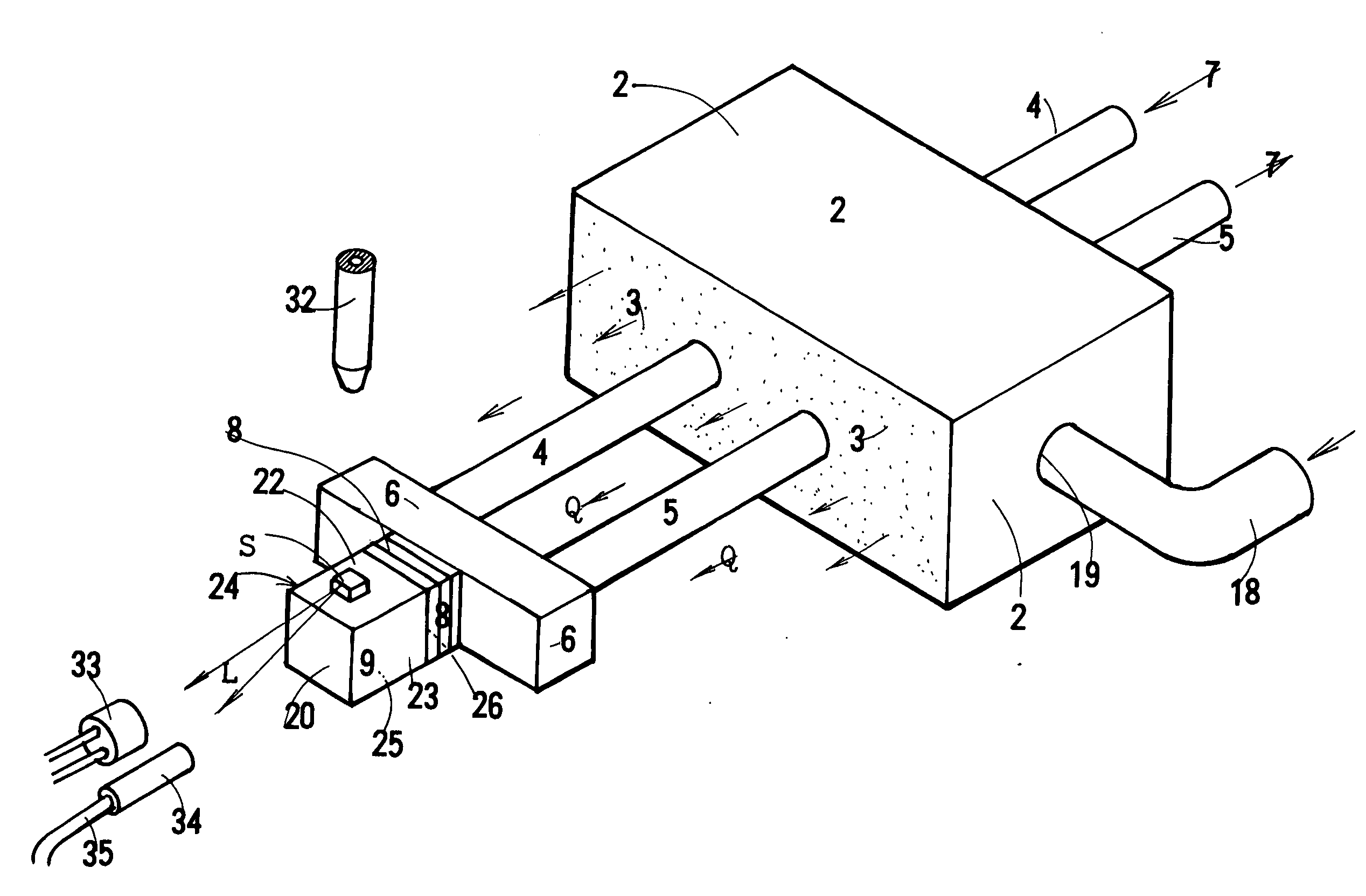
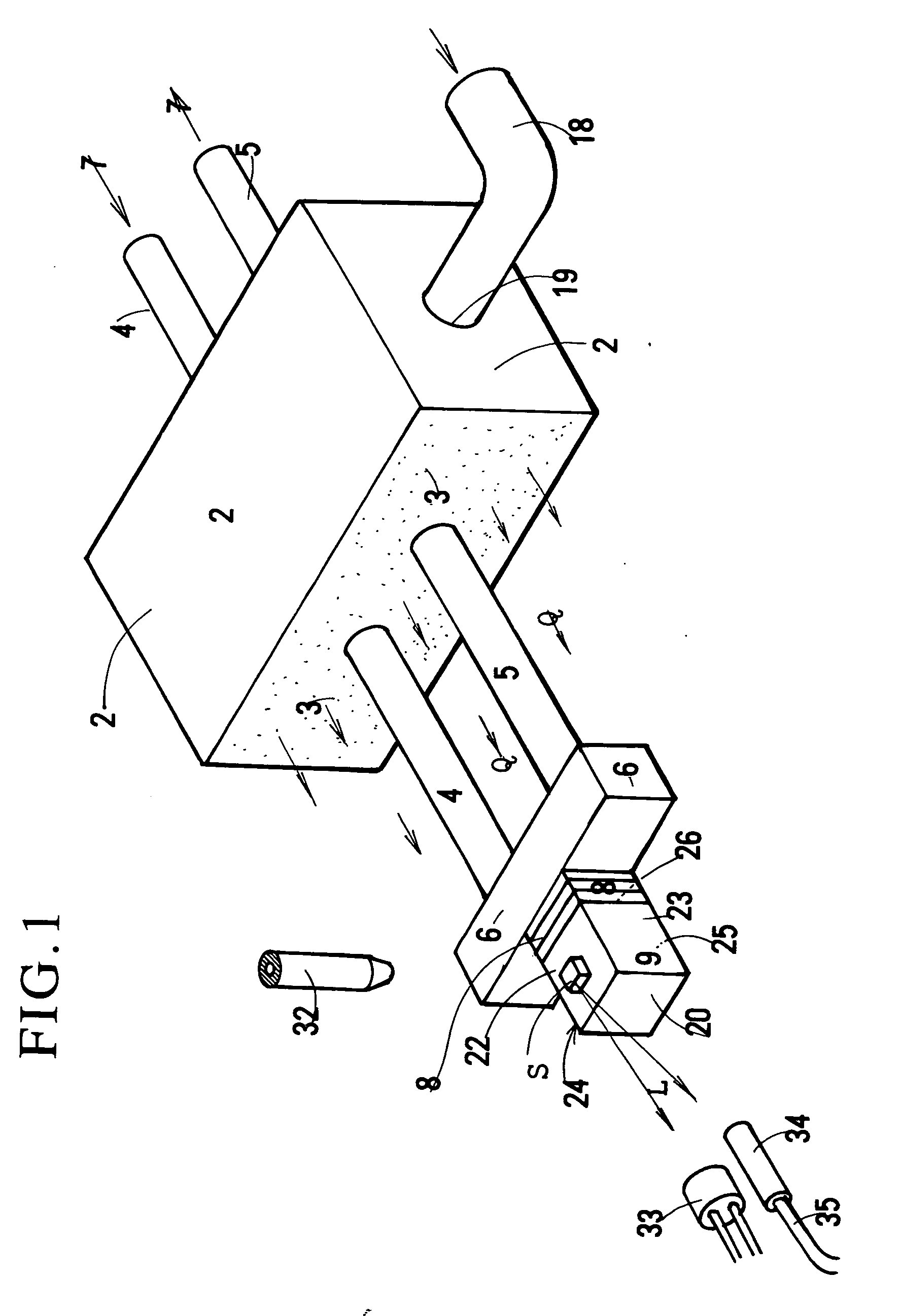
[0054]FIG. 1 is a perspective view of a low temperature characteristic inspection device as Embodiment 1 of the present invention in a state of ridding of shield casing. In reality the shield casing encapsulates inner parts. FIG. 1 omits the shield casing for clarifying the inner structure. FIG. 2 is a perspective view of the whole of Embodiment 1 having the shield casing. FIG. 3 is a vertically sectioned view of the forepart of Embodiment 1 for showing a step of fetching an unexamined chip to an inspecting stage via an opening by a collet and a step of removing an examined chip from the inspecting stage via the opening by the collet. FIG. 4 is a vertical sectioned view of the forefront for showing a step of bringing a probe into contact with the chip, supplying a driving current and observing light emitted from the chip via the front opening. FIG. 5 is a horizontally-sectioned view of Embodiment 1 for showing flows of a liqui...

embodiment 2

Two Openings; Top Opening and Fore Opening; FIG. 6

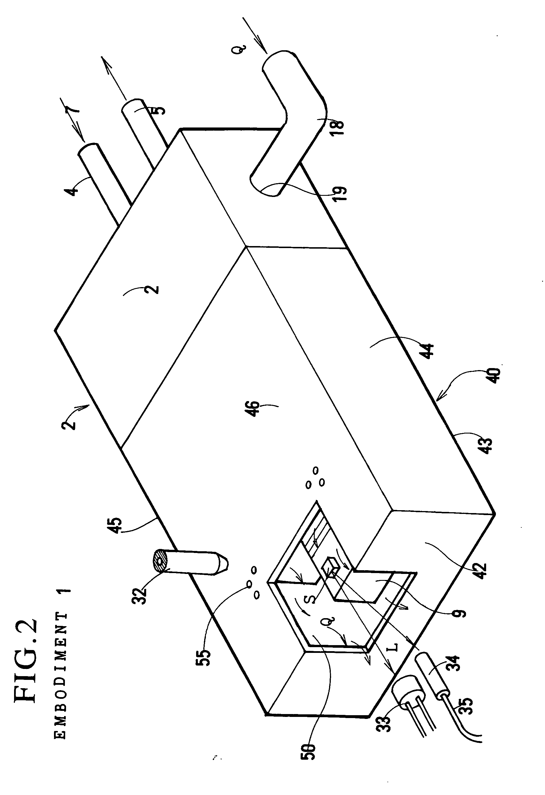
[0073]FIG. 6 shows a perspective view of a low temperature characteristic inspection device as Embodiment 2 of the present invention. Instead of one, two openings are perforated on the shield casing. Embodiment 2 has a top opening 52 for loading chips to the stage or unloading chips from the stage and a fore opening 53 for allowing inspection light to go into or go out of the shield casing. The total area of openings is smaller than Embodiment 1. Narrower openings enable Embodiment 2 to raise the pressure of dry air in the shield casing, to alleviate dry air consumption and to give an inspection device of lower cost than Embodiment 1.


PUM


Abstract

Optoelectronic properties of optical communication LEDs, LDs and PDs should be examined in a wide range of temperatures between −40° C. and +85° C. Low temperature photocharacteristics of as-chip devices are tested by preparing an inspection stage cooled at a low temperature encapsulated in a shield casing with a front opening, conveying a chip of LD, LED or PD by a collet via the opening, placing the chip on the cold stage, blowing the stage and chip with cool dry air for preventing the chip from wetting, touching the chip by a probe, applying a current / voltage to the chip, examining emission / detection of the chip and taking the chip off via the opening by the collet.

Description

RELATED APPLICATIONS [0001] This application claims priority to Japanese Patent Application No. 2005-357072 filed Dec. 12, 2005. BRIEF DESCRIPTION OF THE INVENTION [0002] This invention relates to a low-temperature characteristic inspection device which is capable of examining operation characteristics of optoelectronic semiconductor devices at an as-chip step at low temperatures. Normal operation is required of semiconductor devices in a wide temperature range from −40° C. to +85° C. Guarantee of good operation in the wide range of temperatures should be a requisite for optoelectronic devices, e.g., light emitting devices and light detecting devices and logical electronic devices as FETs. Light emitting devices mean laser diodes (LDs) and light emitting diodes (LEDs). Light detecting (receiving) devices denote photodiodes (PDs), phototransistors (PTRs) and avalanche photodiodes (APDs). Temperature-dependent characteristics of semiconductor devices should be examined between −40° C....

Claims


Application Information

Patent Timeline
IPC IPC(8): G01R31/02
CPCG01R31/2635H01S5/0014H01S5/02208H01S5/02415H01S5/02423
Inventor KAMAKURA, MITSUTOSHI
Owner SUMITOMO ELECTRIC IND LTD
Features
  • Generate Ideas
  • Intellectual Property
  • Life Sciences
  • Materials
  • Tech Scout
  • Unparalleled Data Quality
  • Higher Quality Content
  • 60% Fewer Hallucinations
Learn More