
Variable gain amplifier

a gain amplifier and variable gain technology, applied in the direction of gain control, volume compression/expansion having semiconductor devices, amplification control device circuits, etc., can solve the problems of large design area, large noise factor, complicated circuit, etc., to improve the noise factor, widen the variable gain range, and reduce current consumption

Active Publication Date: 2007-06-14
ELECTRONICS & TELECOMM RES INST
View PDF9 Cites 2 Cited by
  • Summary
  • Abstract
  • Description
  • Claims
  • Application Information

AI Technical Summary

Benefits of technology

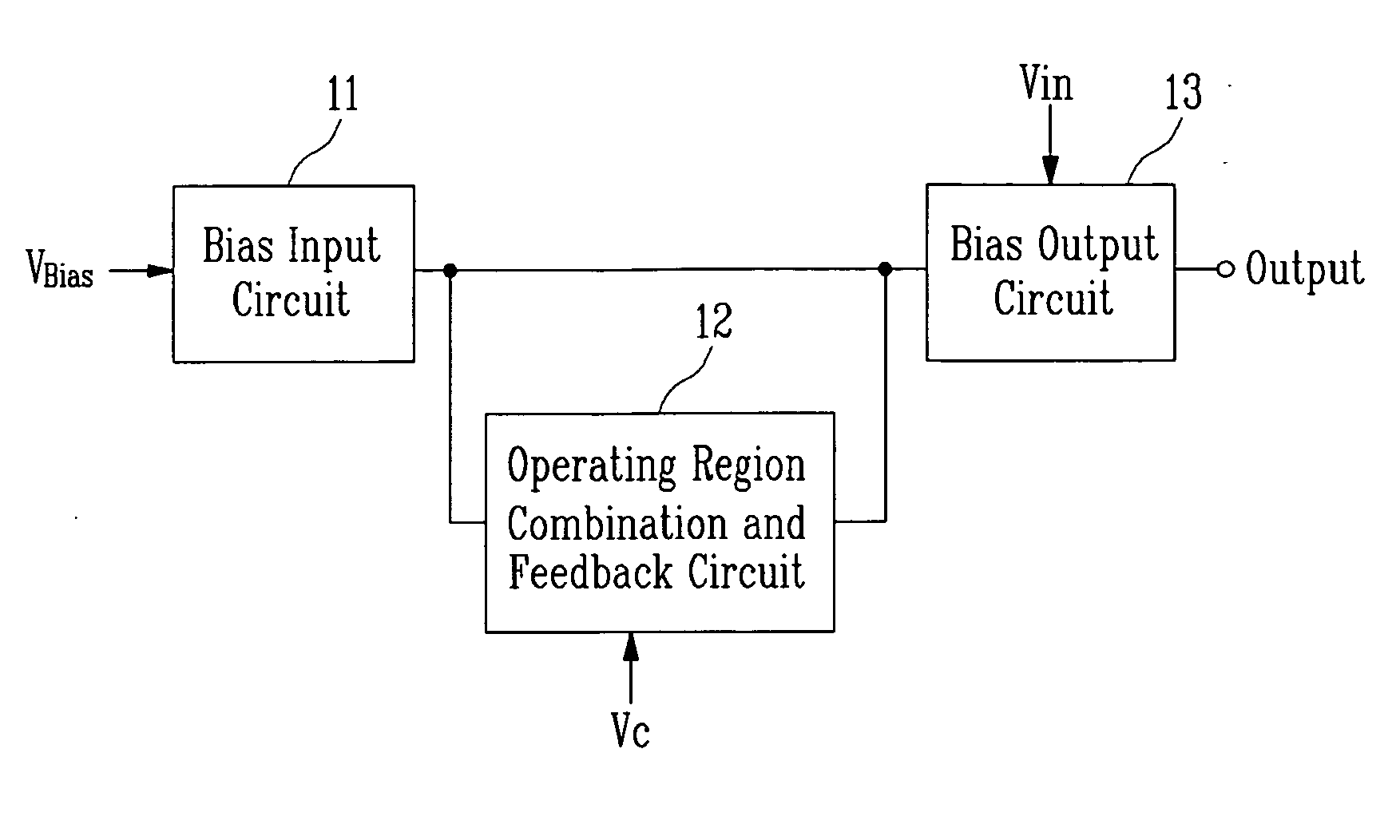
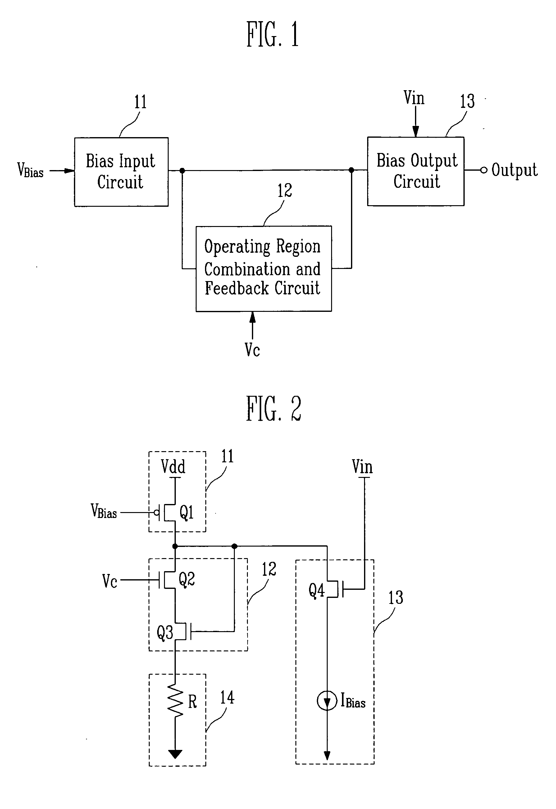
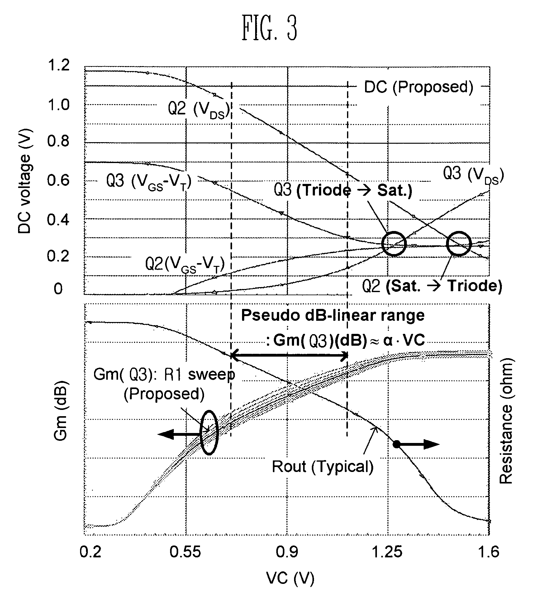
[0008] The present invention is directed to a complementary metal oxide semiconductor (CMOS) variable gain amplifier, which combines an operation region of the amplifier varied between a saturation region and a triode region while forming a feedback loop within a combination circuit, thereby providing a wider variable gain range in the same control voltage variation range, reducing current consumption, improving a noise factor, and considerably reducing a design area, compared to a conventional CMOS variable gain amplifier.

Problems solved by technology

However, unlike the variable gain amplifier using the BJT, the CMOS variable gain amplifier has many transistors, and thus has a complicated circuit, high current consumption, a large noise factor, and a considerably large design area.

Method used


Image

  • Variable gain amplifier
  • Variable gain amplifier
  • Variable gain amplifier

Examples


Embodiment Construction

[0022] Hereinafter, exemplary embodiments of the present invention will be described in detail. However, the present invention is not limited to the exemplary embodiments disclosed below, and can be implemented in various modified forms. Therefore, the present exemplary embodiments are provided for complete disclosure of the present invention and to fully inform the scope of the present invention to those of ordinary skill in the art.

[0023]FIG. 1 is a block diagram illustrating a basic construction of a complementary metal oxide semiconductor (CMOS) variable gain amplifier according to the present invention.

[0024] Basically, the linear-in-dB CMOS variable gain amplifier according to the present invention is to obtain a wider variable gain range by combination of a principle of obtaining a decibel-linear characteristic in a saturation region and a principle of obtaining a decibel-linear characteristic in a triode region. Compared to a conventional CMOS variable gain amplifier, the ...


PUM


Abstract

A complementary metal oxide semiconductor (CMOS) variable gain amplifier has a wider decibel-linear gain variation characteristic with respect to a control voltage when a signal is amplified. The variable gain amplifier includes: a bias input circuit for supplying a current corresponding to a bias voltage; an operation region combination and feedback circuit connected to the bias input circuit and combining at least two amplifiers by feedback in response to a control voltage, each amplifier having a decibel-linear characteristic in saturation and triode regions of a complementary metal oxide semiconductor (CMOS); and a bias output circuit connected to the bias input circuit, and outputting bias current controlled by the operation region combination and feedback circuit.

Description

CROSS-REFERENCE TO RELATED APPLICATION [0001] This application claims priority to and the benefit of Korean Patent Application No. 2005-121442, filed Dec. 12, 2005, the disclosure of which is incorporated herein by reference in its entirety. BACKGROUND [0002] 1. Field of the Invention [0003] The present invention relates to a variable gain amplifier (VGA), and more particularly, to a complementary metal oxide semiconductor (CMOS) variable gain amplifier having a wider variable gain range than a conventional VGA in the same control voltage variation range. [0004] 2. Discussion of Related Art [0005] In general, in a radio frequency (RF) communication transceiver, a receiver has a variable gain amplifier for producing, according to the magnitude of an input signal, a constant signal-to-noise (SNR) characteristic. The variable gain amplifier allows the input signal, whose magnitude in decibels (dB) varies with a distance, to fix the magnitude of a final analog signal of the receiver. Fu...

Claims


Application Information

Patent Timeline
Patent Type & Authority Applications(United States)
IPC IPC(8): H03G3/10
CPCH03F1/342H03F3/211H03F3/45206H03F3/45659H03F2200/15H03F2203/21154H03F2203/45008H03F2203/45302H03G1/007H03G7/06H03F3/45
Inventor HAN, SEON HOYU, HYUN KYU
Owner ELECTRONICS & TELECOMM RES INST
Learn More