Semiconductor Device, and Display Device and Electronic Device Utilizing the Same

a technology of semiconductor devices and electronic devices, applied in the direction of identification means, pulse techniques, instruments, etc., can solve the problems of reducing size and weight, and it is difficult to reduce manufacturing costs to the level sufficiently low, so as to reduce manufacturing costs, prevent the amplitude of output signals from being decreased, and reduce the effect of amplitud

Active Publication Date: 2007-06-14
SEMICON ENERGY LAB CO LTD
View PDF60 Cites 37 Cited by
  • Summary
  • Abstract
  • Description
  • Claims
  • Application Information

AI Technical Summary

Benefits of technology

[0036] By turning OFF the diode-connected transistor, the gate terminal of the first transistor is brought into a floating state. At this time, the first transistor is ON, and its gate-source voltage is stored in a capacitor (gate capacitance of the transistor). Subsequently, when a potential at the source terminal of the first transistor is increased, a potential at the gate terminal of the first transistor is increased as well due to bootstrap effect. As a result, the amplitude of an output signal is prevented from being decreased.
[0040] By turning OFF the diode-connected transistor as the second rectifying element, a potential at the gate terminal of the first transistor is prevented from dropping to a large degree. As a result, the amplitude of an output signal is prevented from being decreased.
[0042] That is, by adopting transistors having the same conductivity for both the first transistor and the diode-connected transistor, all the transistors configuring the circuit can have the same conductivity. As a result, cost reduction can be achieved.
[0044] That is, by adopting transistors having the same conductivity for both the first transistor and the diode-connected transistor as the second rectifying element, the threshold voltage of each transistor can be set roughly the same. Since the threshold voltage of the first transistor is almost equal to that of the diode-connected transistor as the second rectifying element, it is prevented that current leaks when the first transistor is required to be turned OFF.
[0048] According to the configuration of the invention, either terminal of a capacitor configuring a bootstrap circuit is easily brought into a floating state. As a result, the amplitude of an output signal is prevented from being decreased. In addition, even when the amplitude of an input signal is small, either terminal of the capacitor configuring the bootstrap circuit can be brought into a floating state. Therefore, the amplitude of an output signal is prevented from being decreased. Further, as the circuit can be configured by using transistors of only one conductivity, the manufacturing cost can be reduced.

Problems solved by technology

As mobile electronic devices are reduced in size and weight, demand for a display device using a self-light emitting element and a liquid crystal element and the like such as an organic EL element, an FED (Field Emission Display), and an element used for a liquid crystal display is rapidly increasing; however, from the viewpoint of the yield and the like, it is difficult to reduce the manufacturing cost to the level sufficiently low since the great many number of TFTs are required.
However, there is the following problem in this case. FIG. 9C shows the waveform of the output from the TFT load-type inverter circuit.

Method used


Image

  • Semiconductor Device, and Display Device and Electronic Device Utilizing the Same
  • Semiconductor Device, and Display Device and Electronic Device Utilizing the Same
  • Semiconductor Device, and Display Device and Electronic Device Utilizing the Same

Examples


embodiment mode 1

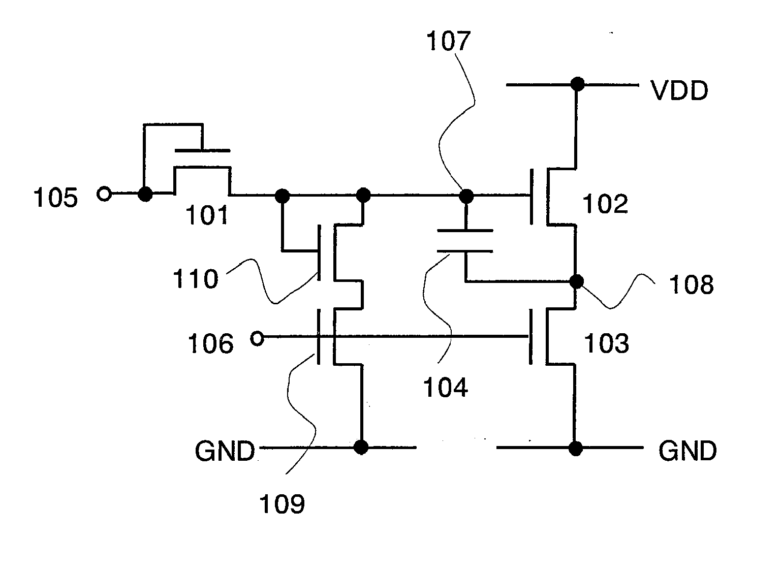
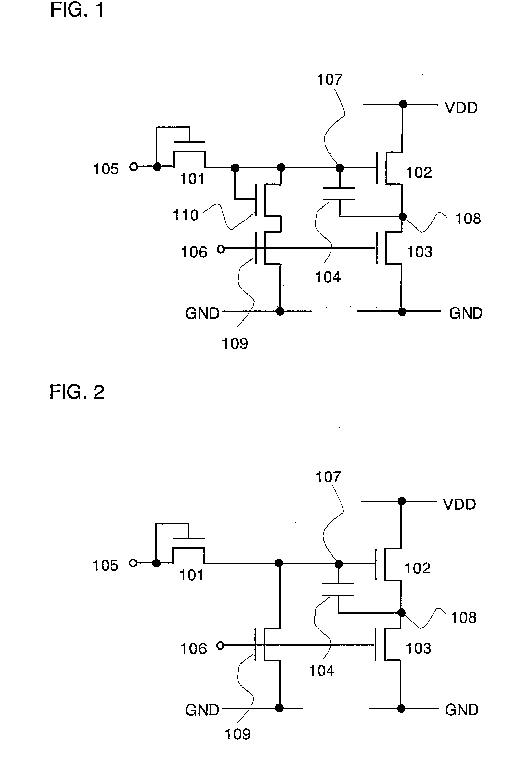
[0084] First, described in this embodiment mode is an inverter circuit for dealing with the second problem as described in the section of the problems to be solved by the invention. That is, described here is the inverter circuit for dealing with the problem that a potential at a certain terminal are not increased sufficiently in the case where a potential of an H signal which is input to an input terminal is lower than a high potential side power supply VDD.

[0085]FIG. 2 shows an inverter circuit in which potentials at terminals 107 and 108 can be increased sufficiently even when a potential of an H signal which is input to an input terminal 105 is lower than a high potential side power supply VDD. The input terminal 105 is connected to the gate terminal of a transistor 102 through a diode-connected transistor 101. Since the transistor 101 is diode connected, its gate terminal is connected to the input terminal 105. Therefore, current can flow in the direction from the terminal 105...

embodiment mode 2

[0104] In Embodiment Mode 1, the inverter circuit for dealing with the second problem described in the section of the problems to be solved by the invention is described. Described in this embodiment mode is an inverter circuit for dealing with the first problem described therein.

[0105] Now, a factor of the first problem is analyzed with reference to the circuit in FIG. 33 again. When an H signal (high potential side power supply VDD) is input to the input terminal 3306 and an L signal (low potential side power supply GND) is input to the input terminal 3305, the potential at the terminal 3307 becomes equal to the potential of the L signal (low potential side power supply GND). That is, the voltage at both ends (potential difference between both ends) of the capacitor 3304 becomes equal to 0 V.

[0106] Next, when an H signal (high potential side power supply VDD) is input to the input terminal 3305 and an L signal (low potential side power supply GND) is input to the input terminal ...

embodiment mode 3

[0120] Described in this embodiment mode is the inverter circuit for dealing with the first and second problems described in the section of the problems to be solved by the invention, which is obtained by modifying the circuit described in Embodiment Mode 1. In this embodiment mode, an inverter circuit for dealing with the first problem is described by modifying the circuit in FIG. 34.

[0121]FIG. 8 shows a modified inverter circuit of FIG. 34. A diode-connected transistor 801 is connected in series to a transistor 3409. It is to be noted that although the transistor 801 is disposed between the drain terminal of the transistor 3409 and the terminal 3407, the invention is not limited to this. For example, it may be connected to the source terminal side of the transistor 3409.

[0122] As described above, by disposing the transistor 801, the potential at the terminal 3407 is prevented from dropping to a large degree. Therefore, the potential at the terminal 3407 is increased quickly. As ...


PUM


Abstract

A semiconductor device having a normal function means is provided, in which the amplitude of an output signal is prevented from being decreased even when a digital circuit using transistors having one conductivity is employed. By turning OFF a diode-connected transistor 101, the gate terminal of a first transistor 102 is brought into a floating state. At this time, the first transistor 102 is ON and its gate-source voltage is stored in a capacitor. Then, when a potential at the source terminal of the first transistor 102 is increased, a potential at the gate terminal of the first transistor 102 is increased as well by bootstrap effect. As a result, the amplitude of an output signal is prevented from being decreased.

Description

INDUSTRIAL FIELD FOR THE INVENTION [0001] The present invention relates to a configuration of a digital circuit. More particularly, the invention relates to a technology for amplifying an output signal even larger by using a bootstrap circuit, and further to a display device, a semiconductor device or an electronic device each using the technology. BACKGROUND ART [0002] In recent years, display devices in which a semiconductor thin film is formed on an insulator such as a glass substrate, in particular active matrix display devices using thin film transistors (hereinafter referred to as TFTs), have been in widespread use in various fields. An active matrix display device using TFTs has several hundred thousand to several million pixels arranged in matrix, and it displays images by controlling the electric charge in each pixel by using a TFT disposed in each pixel. [0003] As a recent technology, the technology relating to poly-silicon TFTs in which a driver circuit is simultaneously ...

Claims


Application Information

Patent Timeline
Patent Type & Authority Applications(United States)
IPC IPC(8): G09G3/36G09F9/30H03K3/356G09G3/00G09G3/20H01L21/8238H03F3/16H03K17/00H03K17/06H03K17/687H03K19/094H03K19/096
CPCG09G2310/0267G09G2310/0275H01L27/1255H01L27/124G09G3/36H03K19/018507G09G5/003G09G3/20G09G2310/0286G09G2310/0291G09G2310/0289G09G2330/021
Inventor KIMURA, HAJIMESHIONOIRI, YUTAKA
Owner SEMICON ENERGY LAB CO LTD
Why Eureka
Try Eureka