
Semiconductor integrated circuit

a technology of integrated circuits and semiconductors, applied in the direction of liquid/fluent solid measurement, instruments, sustainable buildings, etc., can solve the problems of increasing the number of transistors to be mounted, the inability to disregard the leakage current of an soc, and the increase of the leakage current of a single transistor from a physical limitation, so as to achieve high speed operation and reduce the consumption of power. , the effect of high speed

Inactive Publication Date: 2007-06-14
RENESAS ELECTRONICS CORP
View PDF12 Cites 69 Cited by
  • Summary
  • Abstract
  • Description
  • Claims
  • Application Information

AI Technical Summary

Benefits of technology

The patent describes a technique for reducing power consumption and improving processing speed in a semiconductor integrated circuit. It involves using a leading-edge process to integrate a large number of functions into a single chip. However, leakage current can be a problem, so the patent proposes a solution to selectively switch between two processors that have different leakage currents. This allows for a higher operating frequency for certain applications and reduces power consumption for lower operating frequencies. The technique also allows for the use of different processors for different tasks, based on their unique strengths and weaknesses. Overall, the patent provides a way to achieve both reduction in power consumption and enhancement in processing speed in a semiconductor integrated circuit.

Problems solved by technology

When a large number of functions are integrated by using a leading-edge process as described above, it is impossible to disregard a leakage current of an SoC.
The leading-edge process has a tendency that the leakage current of a single transistor is increased from a physical limitation.
Furthermore, the SoC has such a main factor that the number of transistors to be mounted is enormous.
According to such a design, however, there is caused an increase in a leakage current to be a side effect for obtaining a high speed operation.
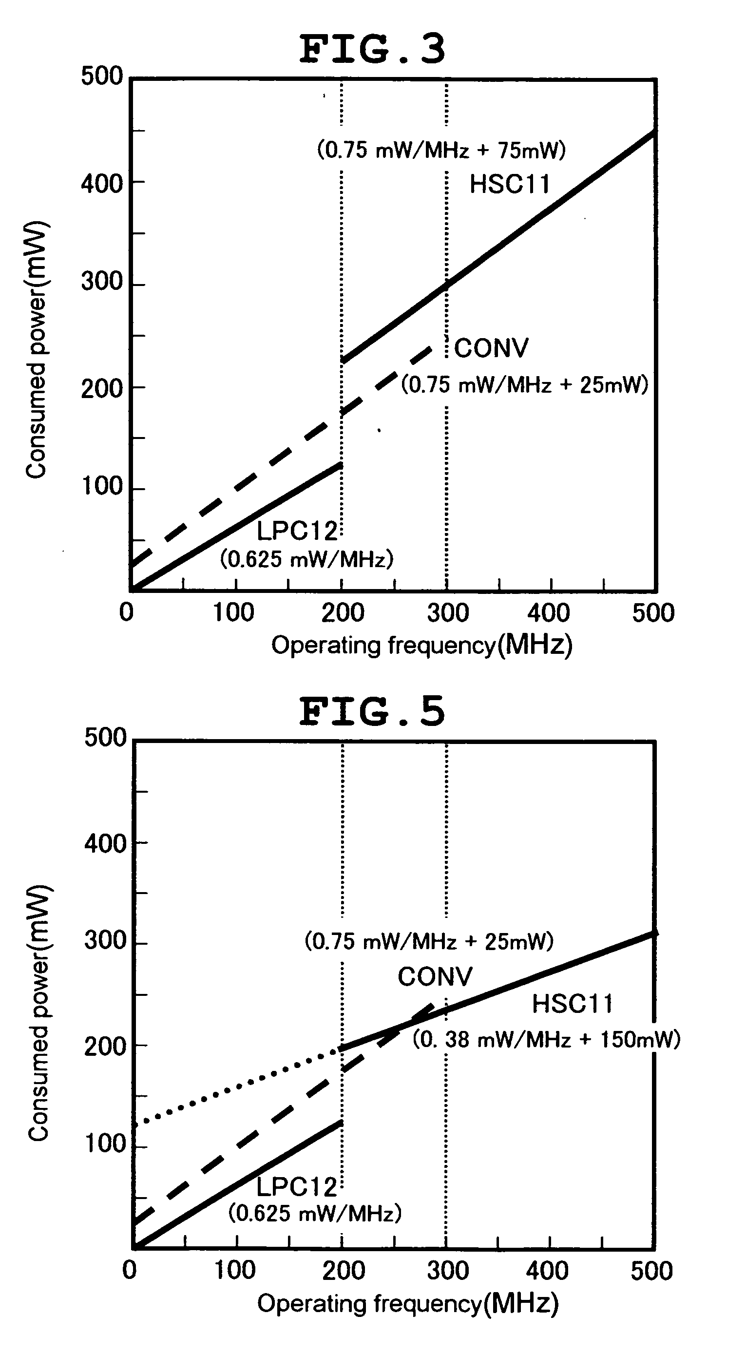
For this reason, there is a problem in that a power consumed by the leakage current is unnecessarily increased in the case in which an operation is carried out at a lower speed.

Method used


Image

  • Semiconductor integrated circuit
  • Semiconductor integrated circuit
  • Semiconductor integrated circuit

Examples


Embodiment Construction

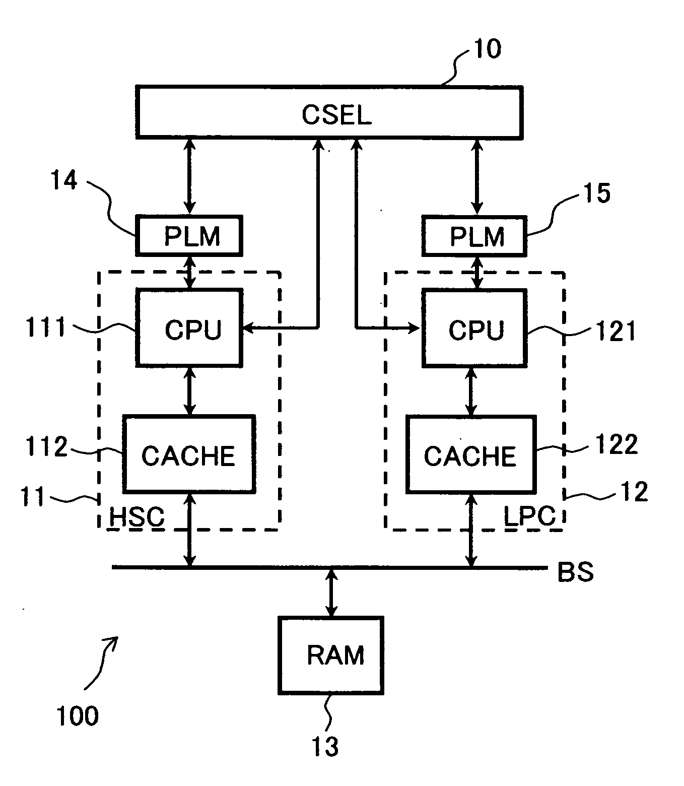
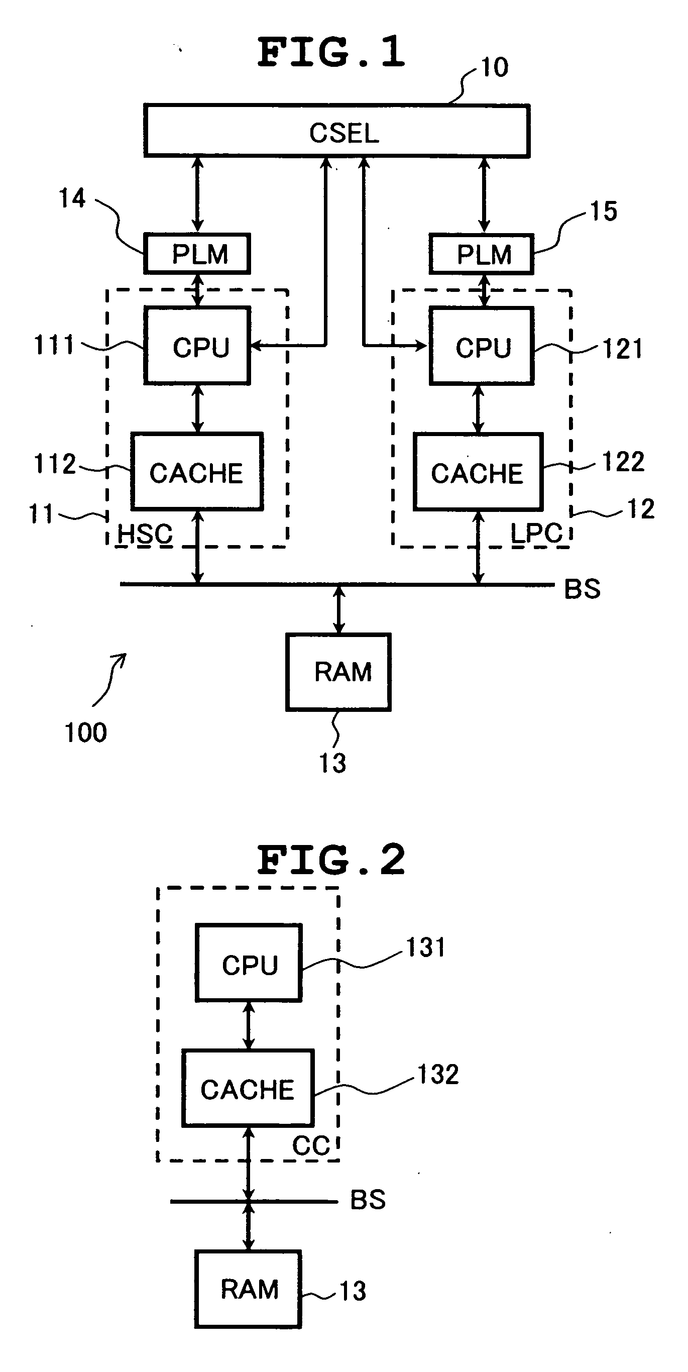
[0047]FIG. 1 shows a microprocessor according to an example of a semiconductor integrated circuit in accordance with the invention.

[0048] A microprocessor 100 shown in FIG. 1 is not particularly restricted but is formed on a semiconductor substrate such as a single crystal silicon substrate by a well-known semiconductor integrated circuit manufacturing technique. The microprocessor 100 has at least two CPU cores, and therefore, is referred to as a multicore. More specifically, the microprocessor 100 includes a high speed processor core (HSC) 11 capable of carrying out a high speed operation and a low power processor core (LPC) 12 capable of carrying out an operation at a low speed and a low power, and information processing is executed by these two cores. The high speed processor core 11 includes a central processing unit (CPU) 111 for a calculation processing and a cache memory (CACHE) 112 for temporarily storing an instruction and data which have high utilization frequencies. Mor...


PUM


Abstract

There are provided a first processor (11) to be operated at a first operating frequency, a second processor (12) in which a leakage current is reduced more greatly than the first processor and which is operated at a lower second operating frequency than the first operating frequency, and a selecting portion (10) capable of selectively switching an executing destination of an application software into the first processor and the second processor corresponding to a demand operating speed of the application software. The first processor and the second processor can execute an identical instruction set, respectively. It is possible to carry out a high speed processing corresponding to the demand operating speed of the application software and to eliminate a dead current caused by a processing at a speed exceeding the demand operating speed of the application software.

Description

CLAIM OF PRIORITY [0001] The present application claims priority from Japanese application JP 2005-344891 filed on Nov. 30, 2005, the content of which is hereby incorporated by reference into this application. FIELD OF THE INVENTION [0002] The present invention relates to a semiconductor integrated circuit, and furthermore, a technique for achieving both a reduction in consumed power and high speed performance therein. BACKGROUND OF THE INVENTION [0003] A demand for enhancing information processing performance to a microprocessor has been increased from year to year, and an enhancement in an operating frequency of the microprocessor has been executed in order to satisfy the demand. In a current semiconductor integrated circuit (LSI), moreover, most of necessary system functions can be integrated in one chip with the progress of a semiconductor process technology. For example, an audio processing IP (Intellectual Property) and an image processing IP can be integrated together with a ...

Claims


Application Information

Patent Timeline
Patent Type & Authority Applications(United States)
IPC IPC(8): G06F1/32G06F1/26
CPCG06F1/3203G06F1/3293H01L21/823462Y02B60/121Y02B60/1217Y02D10/00
Inventor KANNO, YUSUKEMIZUNO, HIROYUKIIRIE, NAOHIKO
Owner RENESAS ELECTRONICS CORP
Learn More