Low defect group III nitride films useful for electronic and optoelectronic devices and methods for making the same

a technology of nitride films and gan films, which is applied in the direction of polycrystalline material growth, chemically reactive gas growth, crystal growth process, etc., can solve the problems of large number of crystal defects in the gan film and active device layer, unsuitable lifetime, and the dislocation density has a detrimental effect on the performance and lifetime of the device, so as to promote the formation of pits

Inactive Publication Date: 2007-06-21
KYMA TECH
View PDF59 Cites 78 Cited by
  • Summary
  • Abstract
  • Description
  • Claims
  • Application Information

AI Technical Summary

Benefits of technology

[0018] According to another implementation, low-defect single-crystal gallium nitride (GaN) on substrate structure is provided. The structure includes a substrate, an epitaxial aluminum nitride (AlN) layer on the substrate, and a GaN film on the substrate. The GaN film includes a first epitaxial GaN growth layer and a second epitaxial GaN growth layer. The first epitaxial GaN layer is grown on the AlN layer under a growth condition that promotes the formation of pits, and after growing the first GaN layer the GaN film surface morphology is rough and pitted. The second epitaxial GaN is grown on the first GaN layer by HVPE under a growth condition that promotes filling of the pits formed, and after growing the second GaN layer the GaN film surface morphology is essentially pit-free.

Problems solved by technology

Most of the III-V nitride devices are grown on foreign substrates such as sapphire (Al2O3) and silicon carbide (SiC) because of the lack of available low-cost, high-quality, large-area native substrates such as GaN substrates.
Because of the lattice mismatch between gallium nitride and the non-native substrate, there is a large number of crystal defects in the GaN film and active device layer.
Despite the high defect density of LEDs grown on these substrates, commercial low-power blue / white LEDs have long lifetimes suitable for some applications.
For LEDs based on an AlGaN active layer operating at the deeper UV range, it is also found that dislocation density has a detrimental effect on the performance and lifetime of the devices.
However, the distribution of the threading dislocation density is not uniform.
The manufacturing cost of the prior-art low defect density GaN film based on MOCVD is high due to multiple growth and photolithographic steps.
The high cost of the film also increases the overall manufacturing cost of end products such as UV LEDs.

Method used


Image

  • Low defect group III nitride films useful for electronic and optoelectronic devices and methods for making the same
  • Low defect group III nitride films useful for electronic and optoelectronic devices and methods for making the same
  • Low defect group III nitride films useful for electronic and optoelectronic devices and methods for making the same

Examples


example 1

Low-Defect GaN Film Growth

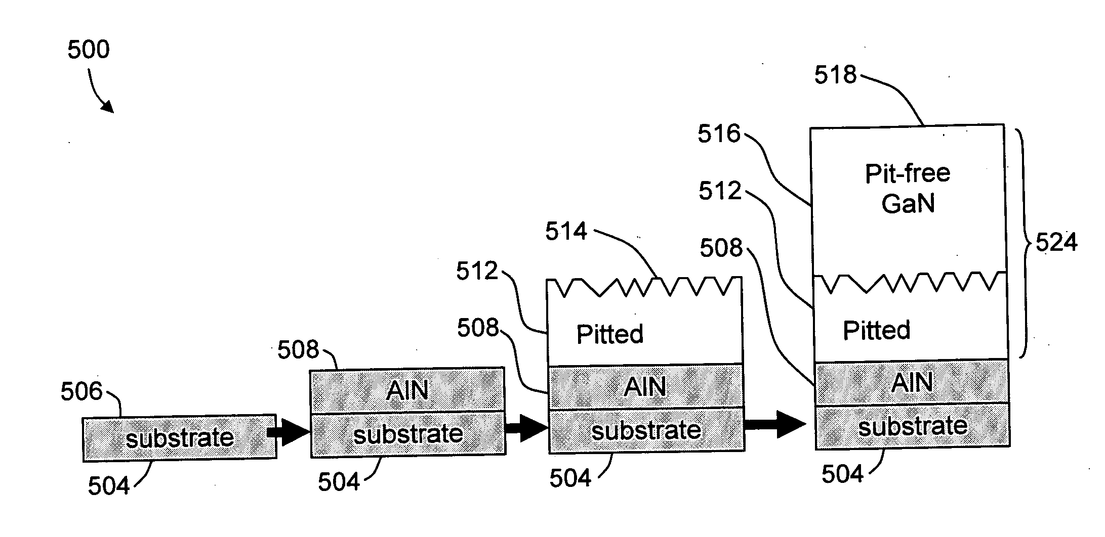
[0071] In this example, we illustrate the growth of a high-quality, low-defect GaN film suitable for the further growth of electronic and optoelectronic devices. A 2″-diameter, 430-micron thick sapphire was used as the starting substrate. Using the sputtering method disclosed in U.S. Pat. No. 6,784,085, an AlN layer approximately 0.7 μm thick was grown on the sapphire substrate for use as a template layer for the HVPE GaN growth. X-ray diffraction was used to verify the AlN film was single-crystal. The AlN / sapphire structure was loaded into a vertical HVPE system and the GaN growth was commenced.

[0072] The HVPE GaN film was grown by a two-step method. The GaN film was first grown under conditions of growth rate of approximately 260 microns per hour, growth temperature of 955° C., HCl flow rate of 92 sccm, and NH3 flow rate of 2500 sccm. After growth of approximately 4 minutes under these growth conditions, the growth rate was reduced to approximately 65 m...

example 2

Low-defect GaN Film Growth

[0074] In this example, we illustrate the growth of another high-quality, low-defect GaN film suitable for the further growth of electronic and optoelectronic devices. A 2″-diameter 430-micron thick sapphire was used as the starting substrate. Using the sputtering method disclosed in U.S. Pat. No. 6,784,085, an AlN layer approximately 0.7 μm thick was grown on the sapphire substrate for use as a template layer for the HVPE GaN growth. The AlN / sapphire structure was loaded into a vertical HVPE system and the GaN growth was commenced.

[0075] The HVPE GaN film was grown by a two-step method. The GaN film was first grown under conditions of growth rate of approximately 260 microns per hour, growth temperature of 955° C., HCl flow rate of 92 sccm, and NH3 flow rate of 2500 sccm. After growth of approximately 3 minutes under these growth conditions, the growth rate was reduced to approximately 30 microns per hour by reducing the HCl flow rate to 10 sccm. At the ...

example 3

Low-defect GaN Film Growth with Lapping Treatment

[0076] The GaN film on sapphire obtained from Example 2 is mounted on a stainless steel plate using wax with the GaN film facing the plate. The backside of the sapphire substrate is lapped on a metal lapping plate with 30-micron diamond slurry. After removing approximately 10 microns from the backside of the sapphire substrate, the wafer bow is reduced from approximately 95 microns to approximately 40 microns.


PUM

PropertyMeasurementUnit
thicknessaaaaaaaaaa
thicknessaaaaaaaaaa
thicknessaaaaaaaaaa

Abstract

In a method for making a low-defect single-crystal GaN film, an epitaxial nitride layer is deposited on a substrate. A first GaN layer is grown on the epitaxial nitride layer by HVPE under a growth condition that promotes the formation of pits, wherein after growing the first GaN layer the GaN film surface morphology is rough and pitted. A second GaN layer is grown on the first GaN layer to form a GaN film on the substrate. The second GaN layer is grown by HVPE under a growth condition that promotes filling of the pits, and after growing the second GaN layer the GaN film surface morphology is essentially pit-free. A GaN film having a characteristic dimension of about 2 inches or greater, and a thickness normal ranging from approximately 10 to approximately 250 microns, includes a pit-free surface, the threading dislocation density being less than 1×108 cm−2.

Description

CROSS-REFERENCE TO RELATED APPLICATIONS [0001] This application claims the benefit of U.S. Provisional Patent Application Ser. No. 60 / 749,728, filed Dec. 12, 2005, titled “Bulk Gallium Nitride Crystals and Method of Making the Same;” U.S. Provisional Patent Application Ser. No. 60 / 750,982, filed Dec. 16, 2005, titled “Method of Producing Freestanding Gallium Nitride by Self-Separation;” U.S. Provisional Patent Application Ser. No. 60 / 810,537, filed Jun. 2, 2006, titled “Low Defect GaN Films Useful for Electronic and Optoelectronic Devices and Method of Making the Same;” U.S. Provisional Patent Application Ser. No. 60 / 843,036, filed Sep. 8, 2006, titled “Methods for Making Inclusion-Free Uniform Semi-Insulating Gallium Nitride Substrate;” and U.S. Provisional Patent Application Ser. No. 60 / 847,855, filed Sep. 28, 2006, titled “Method of Producing Single Crystal Gallium Nitride Substrates by HVPE Method Incorporating a Polycrystalline Layer for Yield Enhancement,” the contents of whic...

Claims


Application Information

Patent Timeline
Patent Type & Authority Applications(United States)
IPC IPC(8): H01L31/00H01L21/00
CPCC30B25/02H01L21/02595C30B25/183C30B29/403C30B29/406H01L21/0237H01L21/02389H01L21/0242H01L21/02433H01L21/02458H01L21/02502H01L21/02505H01L21/0254H01L21/02581H01L21/0262H01L33/007H01L29/04H01L29/2003C30B25/18H01L33/30H01L33/32H01L29/0688H01L21/0257H01L21/02631H01L21/02694
Inventor PREBLE, EDWARD A.LIU, LIANGHONGHANSER, ANDREW D.WILLIAMS, N. MARKXU, XUEPING
Owner KYMA TECH
Why Eureka
Try Eureka