Silicon wafer and method for production of silicon wafer

a technology of silicon wafers and silicon wafers, which is applied in the direction of transportation and packaging, rigid containers, packaging, etc., can solve the problems of short life, short life, and reduced gettering ability, so as to prevent device malfunctions and prolong product life

Inactive Publication Date: 2007-06-21
SUMCO TECHXIV
View PDF2 Cites 10 Cited by
  • Summary
  • Abstract
  • Description
  • Claims
  • Application Information

AI Technical Summary

Benefits of technology

[0036] According to the present invention, as shown in FIG. 1, the silicon wafer 1′ is subjected to a nitrogen doping process, the nitrogen being as an element of facilitating BMD precipitation, and also subjected to an extrinsic gettering (EG) treatment, for example, a process of forming a polysilicon layer 3. Therefore, even if the silicon wafer is exposed to heavy metal ions such as copper, nickel or the like during the device manufacturing process, the intrinsic gettering (IG) acts during the the heat treatment, and thus copper and nickel can be captured (see FIG. 2). In addition, since the polysilicon layer 3 is formed as a strain layer, iron and copper can be captured using the polysilicon layer 3 as a strong point for the capture with the action of the extrinsic gettering (EG)(see FIG. 2). Thus, according to the present invention, sufficient gettering of various heavy metal ions such as iron, copper, nickel or the like generated during the device manufacturing process, can be achieved. Therefore, migrations of heavy metal ions such as iron, copper, nickel or the like into the device layer of the silicon wafer 1′ can be avoided, thereby to prevent malfunctions of the device, and to effect a longer product life.

Problems solved by technology

When heavy metal ions such as iron ions or the like are migrated into the device layer of the silicon wafer 1′ during the device manufacturing process, the resultant devices may possibly perform false operations, and as a result may have a short life.
In addition, since higher concentration of boron as dopant results in higher concentration of BMD, the concentration of the BMD in the p / p− silicon wafer 1′ doped with boron of a low concentration is decreased, thereby reducing the gettering ability thereof.
As such, the silicon wafer 1′ doped with boron of a low concentration and having an epitaxial growth film 2 formed thereon has a problem of lower gettering ability.
However, this attempt has a problem that the heat treatment requires a long time, and thus the manufacturing cost of silicon wafer is increased.
On the other hand, since the above-mentioned steps (a) to (c) should be carried out for performing the EG treatment on the silicon wafer 1′, the steps for manufacturing the wafers become complicated, thereby requiring longer time, and thus the manufacturing cost is increased.
However, the situation of insufficient gettering ability has arisen in both the IG that additionally includes the nitrogen doping process and the EG treatment.
This problem has not been solved in the existing circumstances.

Method used


Image

  • Silicon wafer and method for production of silicon wafer
  • Silicon wafer and method for production of silicon wafer
  • Silicon wafer and method for production of silicon wafer

Examples


Embodiment Construction

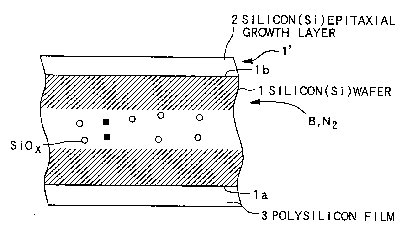
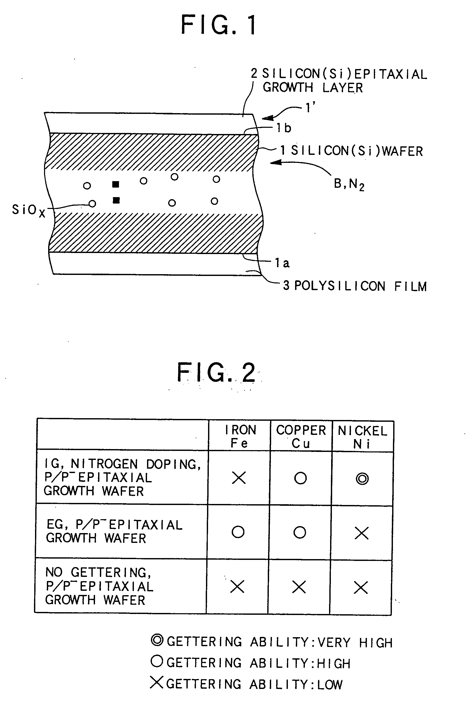
[0042] A semiconductor wafer and a method for manufacturing a semiconductor wafer according to embodiment of the present invention will be described in reference to the accompanying drawings.

[0043] In the embodiment described below, a silicon wafer is employed as the semiconductor wafer.

[0044] In view of the situation in which the gettering abilities is insufficient in both the IG additionally including the nitrogen doping process and the EG treatment, the present inventors have conducted the analysis on the basis of the assumption that the gettering abilities of the EG and the IG vary depending on the type of heavy metal ions. The results of the analysis are shown FIG. 2. Here, the silicon wafer that was analyzed was a p / p− silicon wafer 1′ doped with boron of a low concentration. The term “low concentration” is meant to be a concentration of boron within a range of approximately from 3×10¹⁴ / cm3 to 1×10¹⁶ / cm3 (1 Ω-cm to 15 Ω-cm).

[0045]FIG. 2 shows the results obtained by the ana...


PUM

PropertyMeasurementUnit
concentrationaaaaaaaaaa
diameteraaaaaaaaaa
volumeaaaaaaaaaa

Abstract

A silicon wafer, which has been doped with nitrogen and has been subjected to an extrinsic gettering (EG) treatment, for example, the formation of a polysilicon layer. In the silicon wafer, when the wafer is exposed to an ion of a heavy metal such as copper or nickel in a device manufacturing process, the copper and nickel can be captured by the action of intrinsic gettering (IG) in the course of a heat treatment, and, when a polysilicon layer is formed as a strain layer, iron and copper can be captured by the action of an extrinsic gettering (EG) using the polysilicon as a strong point for the capture.

Description

TECHNOLOGICAL FIELD [0001] The present invention relates to a silicon wafer and a method for manufacturing a silicon wafer. More particularly, the present invention relates to a silicon wafer, which is capable of preventing a contamination of heavy metal ions therein, and a manufacturing method thereof. Background Art [0002] Semiconductor devices are typically manufactured via a device manufacturing process for forming device layers on the surface of the silicon wafer by a thin film, diffusion or the like. [0003]FIG. 3 is a cross sectional view of a silicon wafer 1′ in which an epitaxial growth layer 2 is formed on a silicon wafer substrate 1, assuming that the wafer is a silicon (Si) wafer. [0004] The silicon wafer 1′ is doped with boron B as an impurity (dopant). The silicon wafer 1′ is a p / p− silicon wafer doped with the impurity B of relatively low concentration. Inside the furnace of an epitaxial growth apparatus, feed gases for a thin film such as trichlorosilane (SiHCl3) is s...

Claims


Application Information

Patent Timeline
Patent Type & Authority Applications(United States)
IPC IPC(8): B65D85/00H01L21/322
CPCH01L21/3225H01L21/3221H01L21/20H01L21/322
Inventor IGA, HISAOKITAGAWA, SATOSHI
Owner SUMCO TECHXIV
Why Eureka
Try Eureka