Electroluminescent device containing a butadiene derivative
a technology of butadiene and el, applied in the direction of discharge tube/lamp details, luminescnet screen, discharge tube/lamp details, etc., can solve the problems of inefficiency of the combination of materials, affecting the application of many desirable applications, and limiting the performance of materials, etc., to achieve good luminous yield
- Summary
- Abstract
- Description
- Claims
- Application Information
AI Technical Summary
Benefits of technology
Problems solved by technology
Method used
Image
Examples
example 1
Synthesis of Inv-1
[0158]
[0159] Inv-1 was prepared according to equation 1; the preparation of a similar material is described in US 2003 / 105070. A mixture of Int-A (1.27 g, 3 mmol) and Int-B (0.987 g, 3 mmol) in 10 mL of a mixture of tetrahydrofuran and dimethylforamide (1:1) was added to potassium t-butoxide (0.320 g, 3.3 mmol) in 5 mL of tetrahydrofuran which had been cooled to 0° C. After addition, the temperature was allowed to increase to room temperature while stirring the mixture for 1 h. Water was added and the product was extracted, dried, and evaporated to a solid. The crude product was purified by column chromatography (silica gel, heptane / ethyl acetate eluent) to afford 0.3 g of Inv-1, which sublimed at 240° C.
example 2
Preparation of Devices 1-1 through 1-6
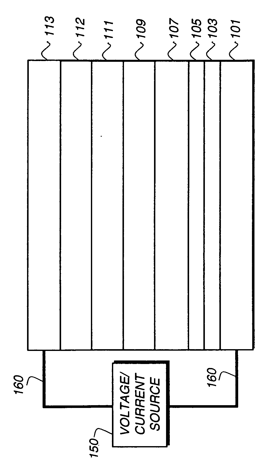
[0160] A series of EL devices (1-1 through 1-6) were constructed in the following manner. [0161] 1. A glass substrate coated with a 25 nm layer of indium-tin oxide (ITO), as the anode, was sequentially ultrasonicated in a commercial detergent, rinsed in deionized water, degreased in toluene vapor and exposed to oxygen plasma for about 1 min. [0162] 2. Over the ITO was deposited a 1 nm fluorocarbon (CFx) hole-injecting layer (HIL) by plasma-assisted deposition of CHF3 as described in U.S. Pat. No. 6,208,075. [0163] 3. Next a layer of hole-transporting material 4,4′-Bis[N-(1-naphthyl)-N-phenylamino]biphenyl (NPB) was deposited to a thickness of 75 nm. [0164] 4. A 20 nm light-emitting layer (LEL) corresponding to 10-(4-biphenyl)-9-(2-naphthyl)anthracene (H-2) and light-emitting material, Inv-1 or L-2 at the level shown in Table 1 was then deposited. [0165] 5. A 35 nm electron-transporting layer (ETL) of tris(8-quinolinolato)aluminum (III) (Alq) wa...
example 3
Preparation of Devices 2-1 through 2-6
[0170] A series of EL devices (1-1 through 1-6) were constructed in the following manner. [0171] 1. A glass substrate coated with an 25 nm layer of indium-tin oxide (ITO), as the anode, was sequentially ultrasonicated in a commercial detergent, rinsed in deionized water, degreased in toluene vapor and exposed to oxygen plasma for about 1 min. [0172] 2. Over the ITO was deposited a 1 nm fluorocarbon (CFx) hole-injecting layer (HIL) by plasma-assisted deposition of CHF3 as described in U.S. Pat. No. 6,208,075. [0173] 7. Next a layer of hole-transporting material 4,4′-Bis[N-(1-naphthyl)-N-phenylamino]biphenyl (NPB) was deposited to a thickness of 75 nm. [0174] 8. A 20 nm light-emitting layer (LEL) corresponding to 10-(4-biphenyl)-9-(2-naphthyl)anthracene (H-2) and light-emitting material Inv-1 or L-47 at the level shown in Table 2 was then deposited. [0175] 9. A 35 nm electron-transporting layer (ETL) of tris(8-quinolinolato)aluminum (III) (Alq) w...
PUM
| Property | Measurement | Unit |
|---|---|---|
| Fraction | aaaaa | aaaaa |
| Fraction | aaaaa | aaaaa |
| Length | aaaaa | aaaaa |
Abstract
Description
Claims
Application Information


