
Electrical device and method of manufacturing electrical devices using film embossing techniques to embed integrated circuits into film

Active Publication Date: 2007-06-21
AVERY DENNISON CORP
View PDF77 Cites 69 Cited by
  • Summary
  • Abstract
  • Description
  • Claims
  • Application Information

AI Technical Summary

Benefits of technology

[0015] According to one aspect of the present invention, a method is provided for embedding a chip in a substrate. The method includes heating the chip and pressing the chip into the substrate. In one embodiment, the chip, heated with thermal radiation, is pressed into a thermoplastic substrate. The heated chip heats the substrate in a localized region thereby softening the thermoplastic substrate and allowing the chip to be embedded therein.
[0019] In one embodiment of the invention, an RFID chip is placed on a substrate with the contacts of the chip facing away from the substrate and the chip and / or the substrate is heated while applying pressure thereby embedding the chip into the substrate. Heating or curing may be achieved in a variety of ways including applying electromagnetic radiation, for example infrared, near infrared, or ultraviolet radiation to the chip and / or web. The chip contacts can be simultaneously coupled with an electrical element, for example conductive leads or an antenna structure which can be preformed on a second substrate which can be laminated to the first substrate. For example, the second substrate that includes the electrical element can be placed on the chip contacts such that the electrical element is facing away from the chip contacts. During the process of embedding and lamanating, the chip contacts penetrate the second substrate and contact the electrical element. The second substrate may be thermoplastic, compressible, or curable. The electrical element on the second substrate can be formed by printing conductive ink. The application of electromagnetic radiation to the second substrate can further cure such ink and enhance its conductivity.
[0020] According to yet another aspect of the present invention, a method of making an RFID transponder is provided comprising: providing a web material, the web material including a continuous conductive element and a compressible substrate layer, forming a recess in the web material by compressing the compressible substrate layer, wherein forming the recess divides the conductive element thereby forming at least two antenna portions, placing a chip in the recess, and coupling the chip to the antenna portions. Forming the recess includes pressing together of the chip and web material and effects the placing and the coupling of the chip.
[0022] In one embodiment, the chip can be used as a forming tool that simultaneously forms a recess in the substrate and embeds the chip in the recess, thereby eliminating the need for the additional steps of separately forming a recess in the substrate and then aligning the chip with the recess prior to its insertion therein.

Problems solved by technology

Pick and place techniques typically involve complex robotic components and control systems that handle only one die at a time.
The larger area reduces the accuracy required for placement of ICs during manufacture while still providing effective electrical connection.
IC placement and mounting are serious limitations for high-speed manufacture.
However, conventional RFID inlay or interposer manufacturing techniques using flip-chip assembly are generally unable to produce devices at a rate fast enough to satisfy demand.
Considerable effort is required to accurately align the chips with the antenna structures often limiting the rate at which devices may be produced.
Thus, the sides of the chips are generally exposed, making the device more vulnerable to damage.
One of the problems with conventional RFID inlay and interposer manufacturing techniques, as well as the RFID devices themselves, is that the chip thickness is greater than the substrate thickness, frequently by a large factor.
Placing the chip onto a film or web substrate creates a bump wherever the chip is located.
Such a bump presents problems for printing equipment that may subsequently print text or graphics onto the label facestock.
In the case of RFID labels or other devices that typically may be printed upon, the uneven surface of the device may interfere with the printing process causing distortion and / or printing errors.

Method used


Image

  • Electrical device and method of manufacturing electrical devices using film embossing techniques to embed integrated circuits into film
  • Electrical device and method of manufacturing electrical devices using film embossing techniques to embed integrated circuits into film
  • Electrical device and method of manufacturing electrical devices using film embossing techniques to embed integrated circuits into film

Examples


Embodiment Construction

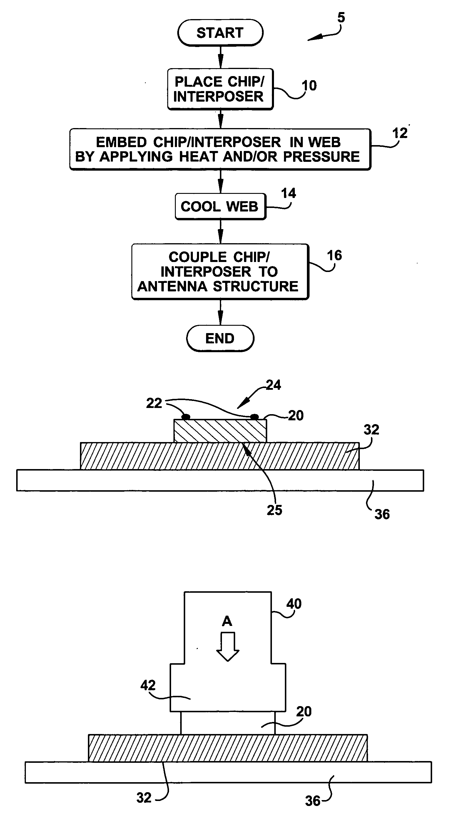
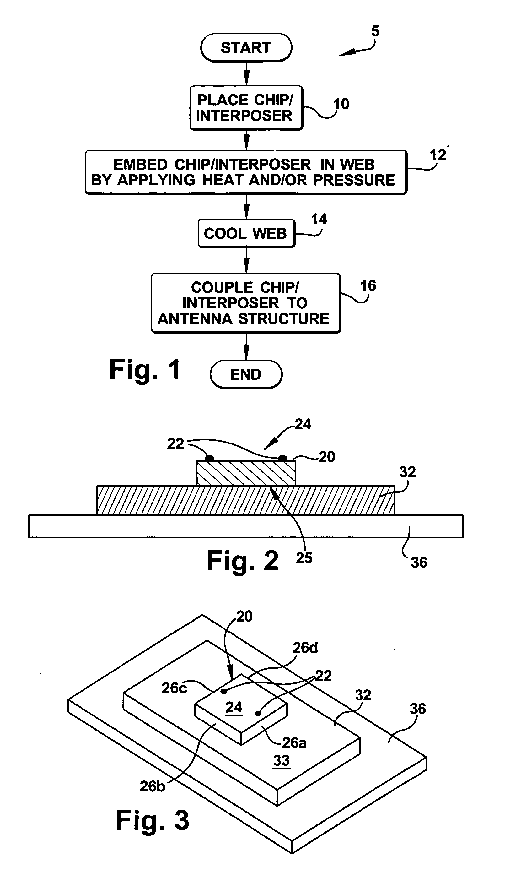
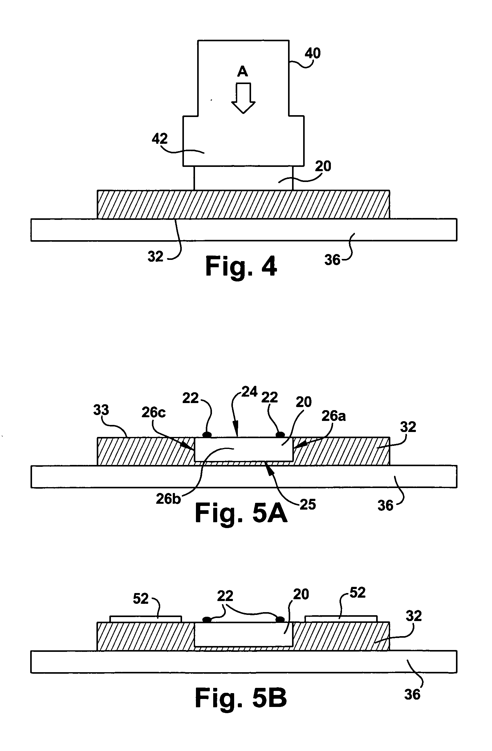
[0055] A method of manufacturing electrical devices is provided wherein a chip or other electrical component is embedded in a substrate. The substrate may be a thermoplastic material capable of deforming around the chip when heat and / or pressure is applied to the substrate. The substrate may include a compressible layer that can be compressed to form a recess into which the chip can be inserted. Once embedded, the chip or electrical component is secured to the web and may be coupled to another electrical component. A method of manufacturing an RFID device is also provided wherein an RFID chip is embedded in a substrate using heat and / or pressure, an antenna structure is applied to the substrate, and the RFID chip and antenna structure are coupled together.

[0056] Referring to FIG. 1, a method 5 of manufacturing electrical devices in web format will be described. It will be appreciated that the electrical devices may be devices other than RFID devices. Similarly, other electrical com...


PUM

PropertyMeasurementUnit
Temperatureaaaaaaaaaa
Pressureaaaaaaaaaa
Electrical conductoraaaaaaaaaa

Abstract

An electrical device and method of making same is provided wherein a chip or other electrical component is embedded in a substrate. The substrate may be a thermoplastic material capable of deforming around the chip and at least partially encasing the chip when heat and / or pressure is applied to the substrate. Electromagnetic radiation such a near infrared radiation can be used to heat the substrate. The substrate may include a compressible layer that can be compressed and / or crushed to form a recess into which the chip can be inserted. Once embedded, the chip or electrical component is secured by the substrate and may be coupled to another electrical component. A method of making an RFID transponder is also provided wherein an RFID chip is embedded in a substrate using heat and / or pressure, an antenna structure is applied to the substrate, and the RFID chip and antenna structure are coupled together.

Description

BACKGROUND OF THE INVENTION [0001] 1. Field of the Invention [0002] The present invention relates generally to electrical devices and to the assembly of electrical devices. More particularly, the present invention relates to the assembly of radio frequency identification (RFID) interposers and / or devices. [0003] 2. Description of the Related Art [0004] Pick and place techniques are often used to assemble electrical devices. Pick and place techniques typically involve complex robotic components and control systems that handle only one die at a time. Such techniques may utilize a manipulator, such as a robotic arm, to remove integrated circuit (IC) chips, or dies, from a wafer of IC chips and place them on a chip carrier, a transport, or directly to a substrate. If not directly mounted, the chips are subsequently mounted onto a substrate with other electrical components, such as antennas, capacitors, resistors, and inductors to form an electrical device. [0005] One type of electrical ...

Claims


Application Information

Patent Timeline
IPC IPC(8): H01L21/00
CPCB29C35/0888B29C43/18H01L2924/07802H01L2924/07811H01L2924/12041H01L2924/014H01L2924/01065B29C2035/0822B29C2035/0827B29C2035/0855B29C2043/3615B32B2519/02G06K19/07745G06K19/07749G06K19/07752H01L21/50H01L23/5389H01L24/19H01L24/97H01L2224/04105H01L2224/20H01L2224/97H01L2924/01002H01L2924/01005H01L2924/01027H01L2924/01029H01L2924/01033H01L2924/01047H01L2924/01059H01L2924/01074H01L2924/01078H01L2924/01082H01L2924/14H01L2924/19041H01L2924/19042H01L2924/19043H01L2924/01019H01L2224/82H01L2924/00H01L2924/181H01L2924/12042H01L2223/6677
Inventor FERGUSON, SCOTT WAYNEMEHRABI, ALIMEHRABI, REZA
Owner AVERY DENNISON CORP
Features
  • Generate Ideas
  • Intellectual Property
  • Life Sciences
  • Materials
  • Tech Scout
  • Unparalleled Data Quality
  • Higher Quality Content
  • 60% Fewer Hallucinations
Learn More