Circuit board assembly with fine electrically connecting structure

a technology of electrical connection and circuit board, which is applied in the direction of electrical connection printed elements, printed circuit details, printed circuits, etc., can solve the problems of affecting the development of packages with a large number of input/output, the function of the packaging substrate, and the limitation of the fabrication method of integrated circuit packaging substrates formed with traces, etc., to achieve high binding intensity, improve the quality of electrical connection, and ensure the effect of electrical connection reliability

Inactive Publication Date: 2007-06-28
PHOENIX PRECISION TECH CORP
View PDF4 Cites 4 Cited by
  • Summary
  • Abstract
  • Description
  • Claims
  • Application Information

AI Technical Summary

Benefits of technology

[0013] In the present invention, the fine electrically connecting structure is a conductive composite material with a net-like bonding configuration, such as an organic composite material characterized with electrical conductivity. Thus, the copper ions in the first and the second circuit layers can migrate to the conductive composite material. As no obvious connecting interfaces exist between the first and the second circuit layers, an interface problem does not occur between the fine electrically connecting structure and the circuit layers, so as to result in a high binding intensity. Furthermore, the performance of electrical connection using the fine electrically connecting structure proposed in the present invention does not require a large dimensioned opening in the dielectric layer. Therefore, the present invention can be applied to a circuit board with fine circuit fabrication while improving the quality of electrical connection of the circuit board and resulting in highly reliable electrical connection.
[0014] The fine electrically connecting structure proposed in the present invention is an organic composite material with a net-like bonding configuration which is characterized with electrical conductivity. Thus, the binding intensity between the fine electrically connecting structure and the dielectric layer can be reinforced by the means of the organic composite material. Moreover, the net-like bonding configuration is highly thermal-tolerated, by which the quality of the fine electrically connecting structure can be effectively controlled to prevent disconnection between circuit layers.

Problems solved by technology

However, the integrated circuit (IC) packaging substrate formed with traces is usually limited by its fabrication method.
In other words, the limitations in the functions of the packaging substrate such as transmission signal of the chip, an improved bandwidth and resistance control impede the development of a package with a large number of input / output (I / O) connections.
Furthermore, the fabrication cost of the substrate is about 20%˜50% of the overall packaging cost.
However, in order to meet the miniaturization requirement of the semiconductor package, when a finer conductive via which has a size smaller than 30 μm is to be fabricated by electroplating, it would be problematical to control the quality of the conductive via due to the difficulties in electroplating techniques.
Therefore, the electrical connection between circuit layers may be adversely influenced, resulting in an unreliable product.

Method used


Image

  • Circuit board assembly with fine electrically connecting structure
  • Circuit board assembly with fine electrically connecting structure
  • Circuit board assembly with fine electrically connecting structure

Examples


Embodiment Construction

[0019] The present invention is described in the following with specific embodiments, so that one skilled in the pertinent art can easily understand other advantages and effects of the present invention from the disclosure of the invention. The present invention may also be implemented and applied according to other embodiments, and the details may be modified based on different views and applications without departing from the spirit of the invention.

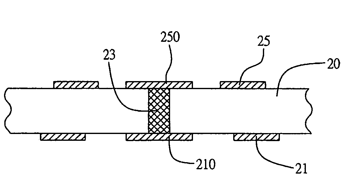
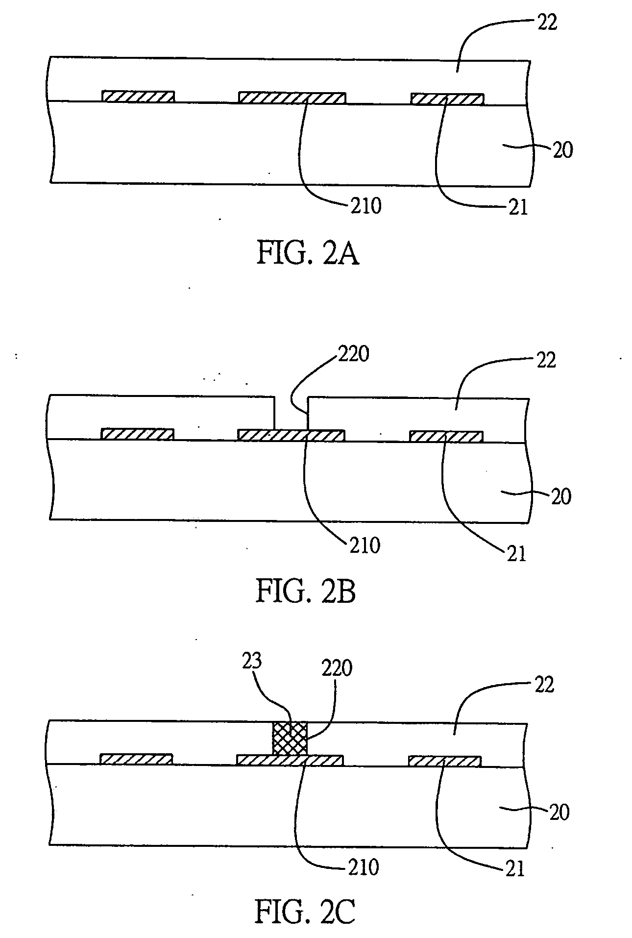
[0020]FIG. 2A to FIG. 2D are cross-sectional views of a circuit board with a fine electrically connecting structure according to the present invention, wherein circuit layers of a circuit board can be electrically connected. In the present embodiment, the fine electrically connecting structure is a conductive via.

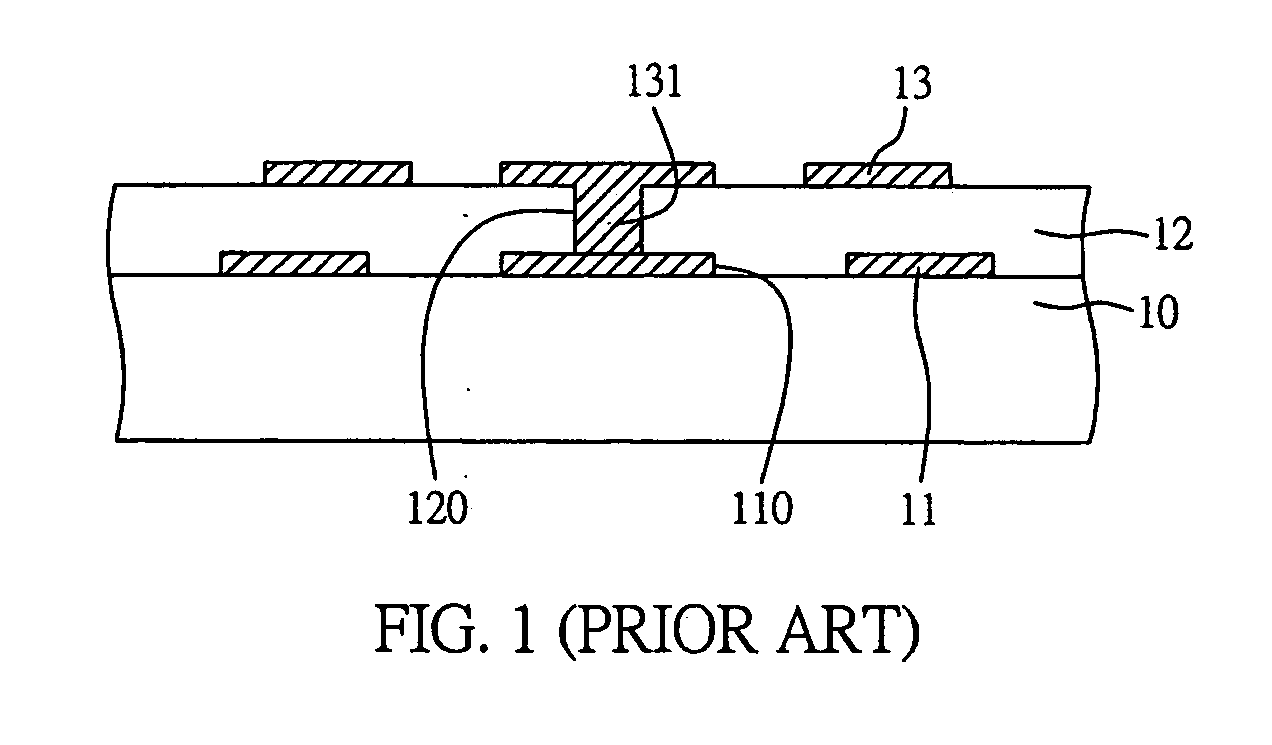
[0021] Referring to FIG. 2A, a circuit board 20 formed with a first circuit layer 21 on a surface thereof is provided. The first circuit layer 21 is formed with at least one electrical pad 210. Further, a dielectric layer 22...


PUM


Abstract

A circuit board assembly with a fine electrically connecting structure is proposed, which includes at least a first circuit layer and at least a dielectric layer formed on surfaces of a circuit board and the first circuit layer. At least one opening is formed penetrating through the dielectric layer for exposing the first circuit layer. Also, at least a fine electrically connecting structure which is electrically connected to the first circuit layer is formed in the opening of the dielectric layer. The fine electrically connecting structure is made of a conductive composite material with a net-like interconnection configuration. At least a second circuit layer which includes at least a circuit and an electrical pad is formed on surfaces of the dielectric layer and the fine electrically connecting structure. By such arrangement, the first circuit layer can be electrically connected to the second circuit layer by the means of the fine electrically connecting structure, so as to achieve electrical connection of fine openings.

Description

CROSS-REFERENCE TO RELATED APPLICATION [0001] This application claims benefit under 35 USC 119 to Taiwan Application No. 094146635, filed Dec. 27, 2005. FIELD OF THE INVENTION [0002] The present invention relates to a circuit board assembly with fine electrically connecting structure, and more particularly, to a circuit board having fine openings with fine electrically connecting structures for electrically connecting interlayer circuits. BACKGROUND OF THE INVENTION [0003] Along with the blooming development of various portable products in the fields of communication, networking and computing, packages such as ball grid array (BGA), flip chip, chip size package (CSP) and multi chip module (MCM) which are characterized with a miniaturized integrated circuit (IC) area, a high density and multiple leads have become the mainstream of the packaging market. Highly effective chips such as a microprocessor, a chip set, a drawing chip and an application-specific integrated circuit (ASIC) are...

Claims


Application Information

Patent Timeline
Patent Type & Authority Applications(United States)
IPC IPC(8): H05K1/11H01R12/04
CPCH05K3/4069H05K3/4644H05K2203/101H05K2203/1461H01R12/523
Inventor HSU, SHIH-PING
Owner PHOENIX PRECISION TECH CORP
Why Eureka
Try Eureka