Pointing device with an integrated optical structure

a technology of optical structure and optical pointing device, which is applied in the direction of instruments, computing, electric digital data processing, etc., can solve the problem that the prism method cannot make parallel light, and achieve the effect of improving optical efficiency, reducing electric power consumption, and high mobility

Inactive Publication Date: 2007-06-28
MOBISOL +1
View PDF6 Cites 92 Cited by
  • Summary
  • Abstract
  • Description
  • Claims
  • Application Information

AI Technical Summary

Benefits of technology

[0014] An object of the present invention is to provide a micro-optical pointing device applicable to a small portable mobile device with high mobility such as a cellular phone and PDA, which can reduce spending of electric power by embodying a pointing device using a lattice type or perceivable pattern as a contact member so as to improve an optical efficiency compared to a method of directly rubbing a finger on a contact member.
[0016] Another object of the present invention is to provide a micro-optical device which can illuminate uniformly a small plane non-perpendicular to the direction of light by adjusting light generated from a light source of a optical device that is designed so that the irradiated lightness is uniform within a irradiation area and becomes parallel light, in illuminating an image acquisition area of a pointing device.
[0017] Another object of the present invention is to provide an integrated two-dimensional pointing device, which can be mounted on a small mobile terminal by integrating and packaging the whole optical and other structures within a small space, and maximize light utilization efficiency by concentrating light parallel so that light from a light source is uniformly irradiated on a definite area and blocking disturbance ray. Technical Solution
[0018] To achieve these objects and other advantages and in accordance with the purpose of the invention, as embodied and broadly described herein, this invention provides a two-dimensional pointing device comprising: a light source emitting light rays to a subject; a contact member comprising a lattice type or perceivable pattern, which reflects an image of the moving subject after receiving light from the light source; a handling surface of image acquisition member, which is positioned on the contact member and has a surface to increase friction force with a finger; an image-formation optical lens, which condenses the light reflected from the contact member and sends the condensed light to an optical sensor; an automatic transfer device which reconveys the contact member moved by the finger; and the optical sensor receiving the image reflected from the optical lens and converting the same into an electronic signal. The contact member having a lattice type or perceivable pattern may be designed so that it can be transferred by an automatic transfer device included in a separate structure. The present invention can reduce power dissipation by forming a handling surface of image acquisition member and a touch sensor over the contact member and making the light source bright only when a finger is contact with the touch sensor. In addition, by blocking light while the pointing device is not used, the present invention prevents a disturbance of user's sight.

Problems solved by technology

However, Choi's portable wireless information terminal adopts a general prism method which irradiates the reflected light onto a contact member after reflecting light from a light source and, therefore, may malfunction because of influx of peripheral disturbance ray into a sensor.
In addition, such a prism method cannot make parallel light.

Method used


Image

  • Pointing device with an integrated optical structure
  • Pointing device with an integrated optical structure
  • Pointing device with an integrated optical structure

Examples


Embodiment Construction

[0037] Further objects and advantages of the invention can be more fully understood from the following detailed description taken in conjunction with the accompanying drawings.

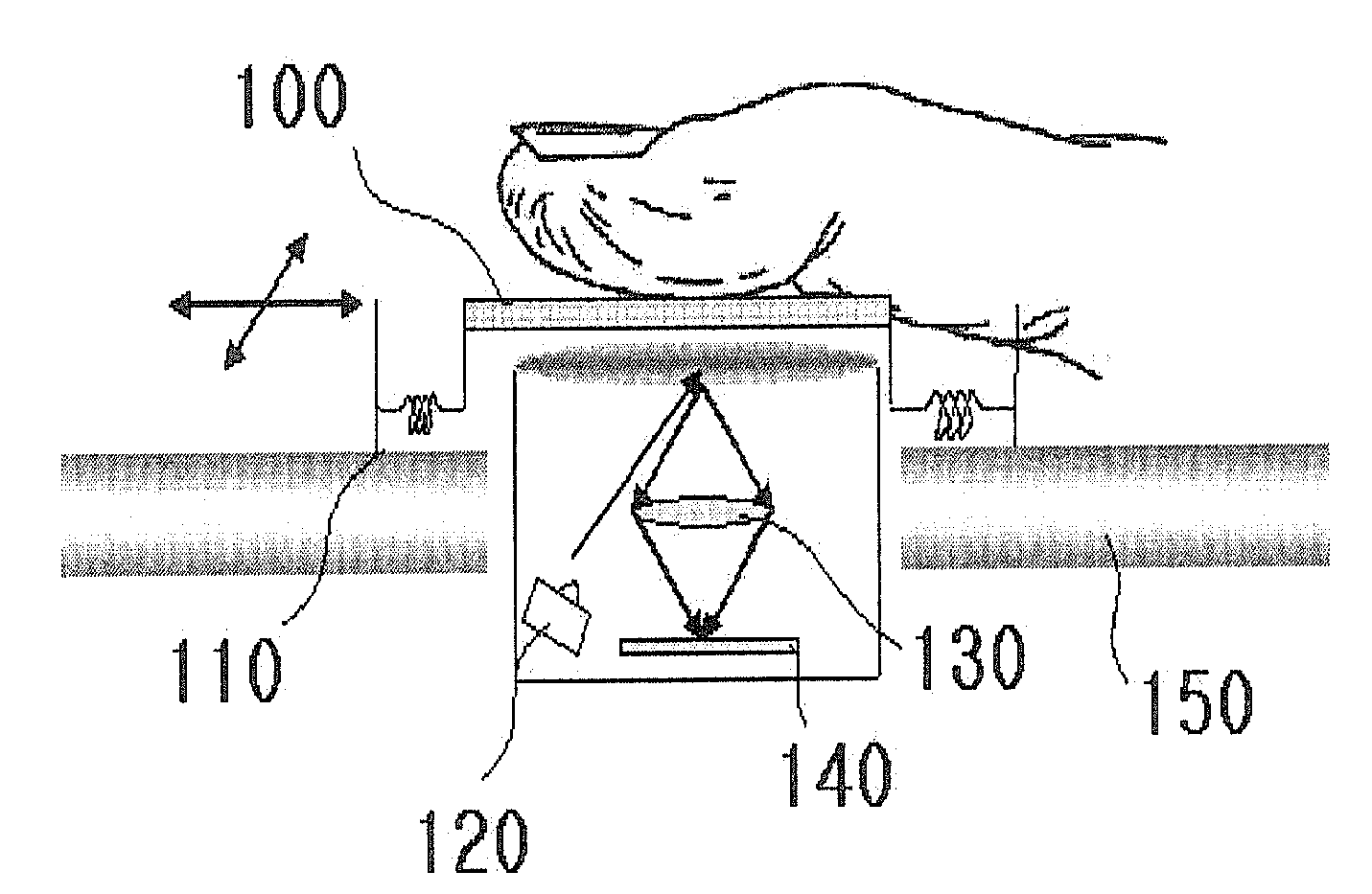
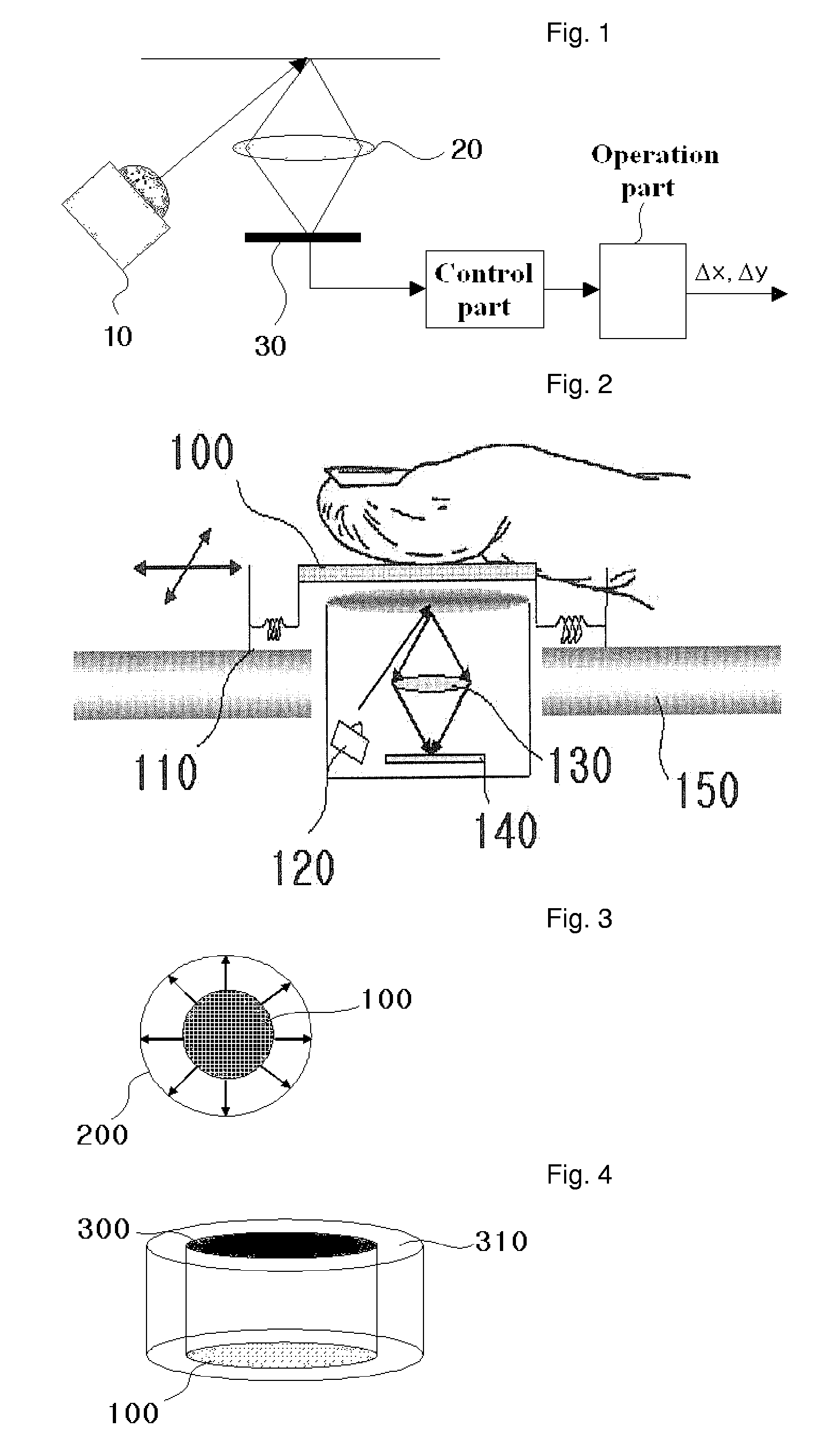
[0038]FIG. 2 is a schematic diagram illustrating an automatic transfer device of a pointing device in accordance with the present invention.

[0039] Referring to FIG. 2, light from a light source (120) is irradiated to a contact member (100). A subject is in contact with the contact member (100). The light reflected from the contact member (100) passes through an image-formation lens (130) to form an image onto an optical sensor (140). Here, the contact member (100) comprises a lattice type or perceivable pattern.

[0040] The contact member (100) may be moved by an automatic transfer device (110) which is installed into a separate structure such as a PCB (150) or key pad of a cellular phone. The automatic transfer device (110) is formed of elastic material such as rubber or silicon, or magnetic material. The co...


PUM


Abstract

The present invention relates to a micro-optical pointing device suitable for mobile terminals such as a cellular phone and PDA. A disclosed pointing device includes a light source emitting light rays to a subject; a contact member comprising a lattice type or perceivable pattern, which reflects an image of the moving subject; and an automatic transfer device restoring the contact member moved by a finger. The pointing device may further include a flip chip containing an image sensor, which converts the acquired image into an electronic signal, and a circuit for signal processing. The pointing device may include an integrated optical structure comprising a condensing lens, a specular surface, a light output part, and an image-formation lens. The pointing device may include a light guide structure that a parallel light prism lens, an image-formation lens, and a mask for blocking disturbance ray are formed into a single part.

Description

TECHNICAL FIELD [0001] The present invention relates to an optical pointing device with an integrated optical structure and, more particularly, a micro-optical pointing device suitable for a mobile device such as a cellular phone and a personal digital assistant (hereinafter referred to as “PDA”), which is applicable to an electronic device requiring a waterproof and dustproof pointing device by forming a microelectronic circuit using a wafer-scale flip chip semiconductor package and integrating the same with an integrated optical structure; can improve optical efficiency by concentrating light from a light source and blocking disturbance ray; can lengthen operating time of a mobile terminal employing secondary batteries by determining whether or not the terminal is used and switching the pointing device into a power saving mode to reduce power dissipation when the mobile terminal is not used; and can be mounted on a small mobile terminal by integrating and packaging optical and oth...

Claims


Application Information

Patent Timeline
Patent Type & Authority Applications(United States)
IPC IPC(8): G09G5/08G06F3/033G06F3/042
CPCG06F3/0421
Inventor JUH, SUNG CHULCHUNG, KYOUNG UNKIM, YOON SOOCHO, KYU DEUKKIM, TAE WOOYONG, DONG JUNGJO, JAE YOUNGOH, SEUNG HAIJUN, SUNHWANG, KYU MIN
Owner MOBISOL
Why Eureka
Try Eureka