Electron emission device, backlight unit (BLU) including the electron emission device, flat display apparatus including the BLU, and method of driving the electron emission device

a technology of electron emission device and backlight unit, which is applied in the direction of discharge tube main electrode, discharge tube luminescnet screen, instruments, etc., can solve the problems of undesirable electron emission through the use of high anode voltage, inability to contribute to light emission by other incident electrons, etc., and achieve high luminous uniformity and luminous efficiency

Inactive Publication Date: 2007-07-05
SAMSUNG SDI CO LTD
View PDF8 Cites 4 Cited by
  • Summary
  • Abstract
  • Description
  • Claims
  • Application Information

AI Technical Summary

Benefits of technology

[0015]The present invention provides an electron emission device which can effectively block an electric field generated by an...

Problems solved by technology

Due to the light emission characteristics of phosphor materials, when light is emitted by an electron that is incident on a phosphor material, other incident electrons cannot contribute to light emission.
Thus, the light emission efficiency is not improved by increasing the number of electr...

Method used


Image

  • Electron emission device, backlight unit (BLU) including the electron emission device, flat display apparatus including the BLU, and method of driving the electron emission device
  • Electron emission device, backlight unit (BLU) including the electron emission device, flat display apparatus including the BLU, and method of driving the electron emission device
  • Electron emission device, backlight unit (BLU) including the electron emission device, flat display apparatus including the BLU, and method of driving the electron emission device

Examples


first embodiment

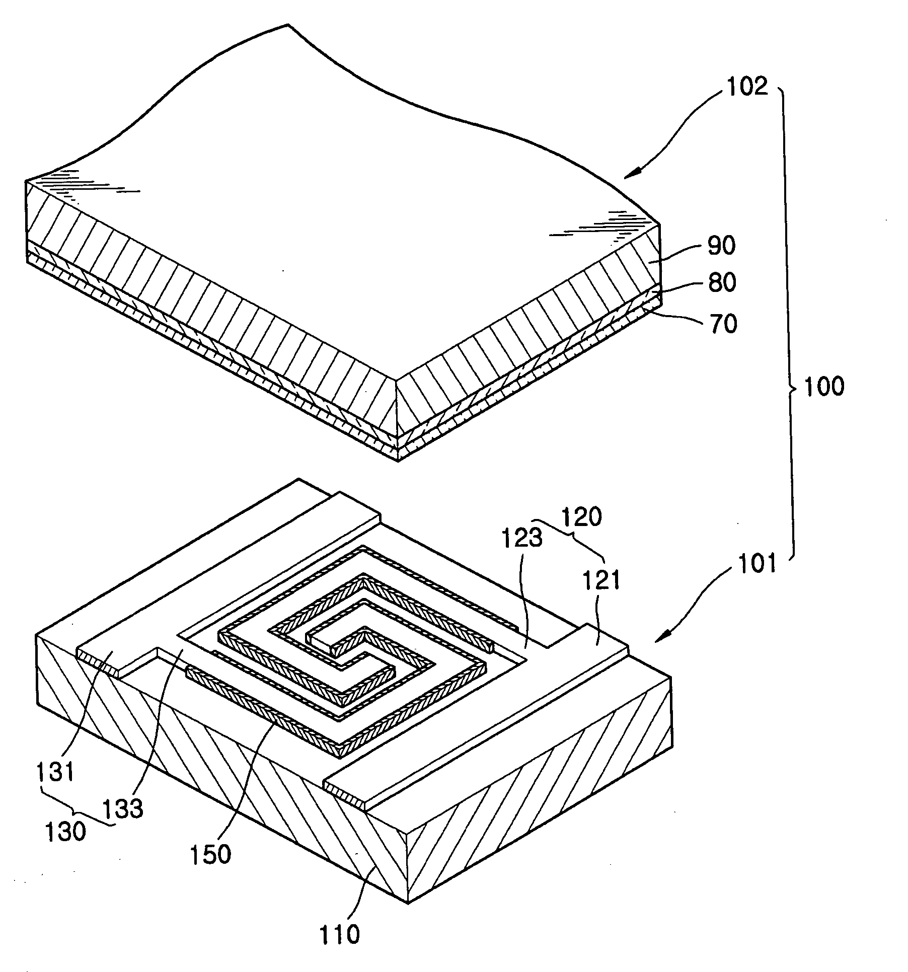
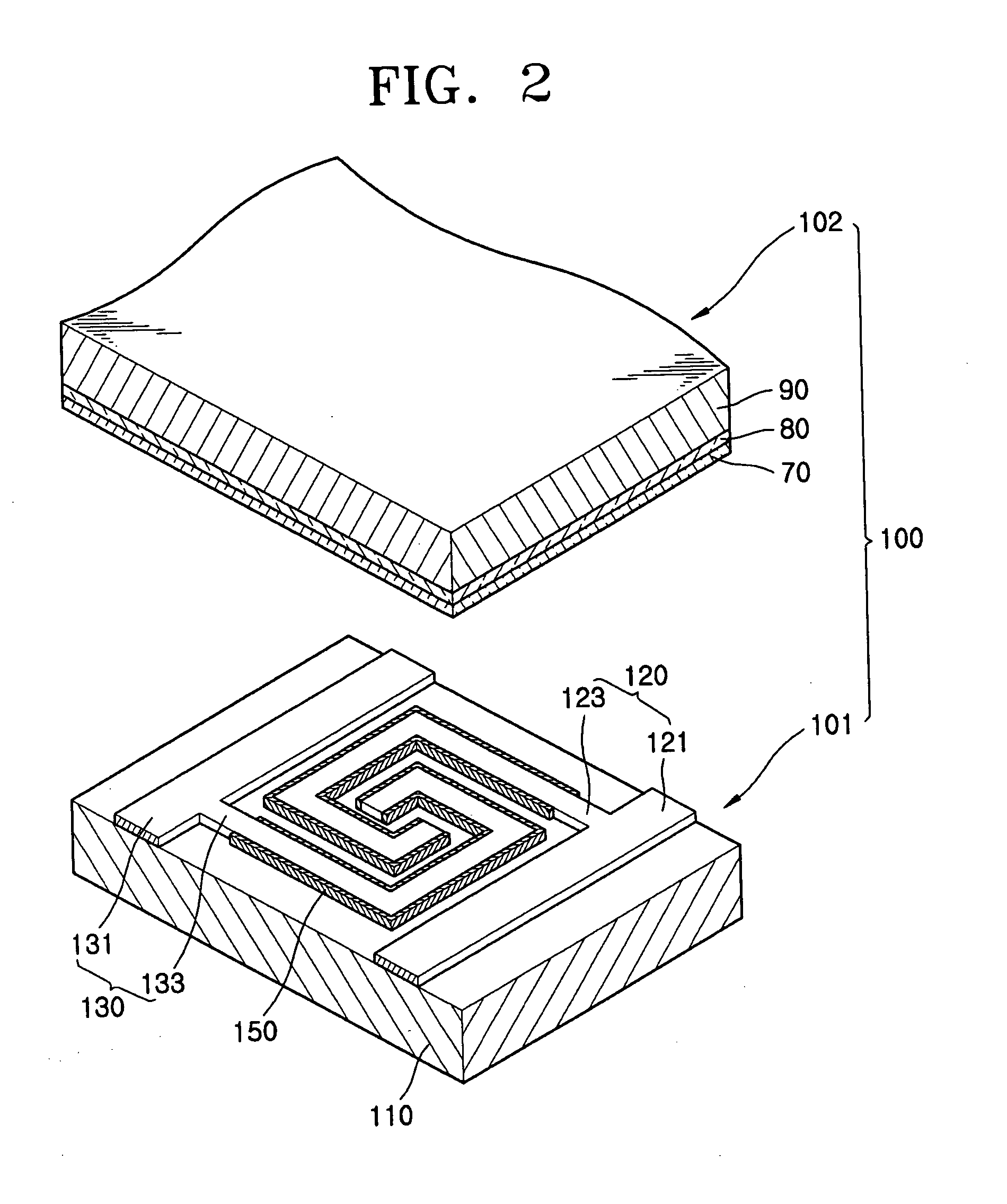
[0057]FIG. 2 is a perspective view of an electron emission device 101 according to a first embodiment of the present invention. FIG. 3 is a plan view of the electron emission device 101 of FIG. 2.

[0058]Referring to FIGS. 2 and 3, the electron emission device 101 according to the first embodiment of the present invention includes a base substrate 110, a first electrode 120, a second electrode 130, and an electron emission source 150.

[0059]The base substrate 110 is a board member having a predetermined thickness, or a glass substrate formed of quartz glass, glass containing a small amount of an impurity such as Na, plate glass, or glass coated with SiO2, aluminum oxide, or a ceramic. If a flexible display apparatus is to be implemented, the base substrate 210 can be formed of a flexible material.

[0060]The first electrode 120 includes a first main electrode portion 121 which extends in one direction on the base substrate 110 and a first auxiliary electrode portion 123 which is formed i...

second embodiment

[0075]FIG. 4 is a perspective view of an electron emission device 201 according to a second embodiment of the present invention. FIG. 5 is a plan view of the electron emission device 201 of FIG. 4.

[0076]Referring to FIGS. 4 and 5, the electron emission device 201 according to the second embodiment of the present invention has the same structure as the electron emission device 101 according to the first embodiment described above, but further includes auxiliary electrodes 122 and 132 on the first and second electrodes 120 and 130. The auxiliary electrodes 122 and 132 can be insulated from the first and second electrodes 120 and 130 by a separate insulating layer or can be electrically connected to the first and second electrodes 120 and 130. Like the first and second electrodes 120 and 130, the auxiliary electrodes 122 and 132 are formed of conductive materials. However, it is not necessary for the auxiliary electrodes 122 and 132 to be formed of the same materials as the first and s...

second embodiments

Modifications of First and Second Embodiments

[0080]FIGS. 6 through 15 are views of modified versions of the electron emission device 101 of FIG. 3 according to the first embodiment of the present invention and the electron emission device 201 of FIGS. 4 an 5 according to the second embodiment of the present invention.

[0081]In FIG. 6, unlike in the electron emission device 201 of FIG. 5 according to the second embodiment of the present invention, an electron emission source 150 is disposed on a second electrode 130 only. In this regard, electrons are emitted from the electron emission source 150 disposed on one of a first electrode 120 and a second electrode 130 to which a negative voltage is supplied, and therefore, the electron emission source 150 need not be disposed on both of the first and second electrodes 120 and 130, and it can be more efficient to form the electron emission source 150 on only one electrode, for example, the second electrode 130 as illustrated in FIG. 6.

[0082...


PUM


Abstract

An electron emission device effectively blocks an electric field generated by an anode, consistently and stably emits electrons at a low gate voltage, and provides a high luminous uniformity and luminous efficiency. In addition, a flat display apparatus using the electron emission device as a backlight unit (BLU) and a method of driving the light emission device are provided. The electron emission device includes: a base substrate; a first electrode including a first main electrode portion arranged on a surface of the base substrate and extending in a predetermined direction and a first auxiliary electrode extending from the first main electrode portion; a second electrode including a second main electrode portion arranged on the surface of the base substrate and separated from the first electrode and extending in a predetermined direction and a second auxiliary electrode extending from the second main electrode portion; and an electron emission source arranged on at least one of the first and second electrodes.

Description

CLAIM OF PRIORITY[0001]This application makes reference to, incorporates the same herein, and claims all benefits accruing under 35 U.S.C.§119 from an application for ELECTRON EMISSION DEVICE, BACK LIGHT UNIT HAVING THE SAME, FLAT DISPLAY APPARATUS HAVING THE SAME, AND METHOD OF DRIVING ELECTRON EMISSION DEVICE earlier filed in the Korean Intellectual Property Office on the 29 of Dec. 2005 and there duly assigned Ser. No. 10-2005-0133417.BACKGROUND OF THE INVENTION[0002]1. Field of the Invention[0003]The present invention relates to an electron emission device, a backlight unit (BLU) including the electron emission device, a flat display apparatus including the BLU, and a method of driving the electron emission device. More particularly, the present invention relates to an electron emission device having a high electron emission efficiency and luminous uniformity, a BLU including the electron emission device, a flat display apparatus including the BLU, and a method of driving the el...

Claims


Application Information

Patent Timeline
IPC IPC(8): H01J63/04H01J1/62
CPCG02F1/133604H01J63/06H01J1/30H01J31/127H01J2329/0405
Inventor CHO, YOUNG-SUKBAE, JAE-WOOKANG, DONG-HYUNJOO, KYU-NAMDO, UI-SONGLIM, IK-CHULZANG, DONG-SIKCHOI, YONG-SOOSON, KYOUNG-CHEON
Owner SAMSUNG SDI CO LTD
Why Eureka
Try Eureka