Method and apparatus for integrated cell handling and measurements

a technology applied in the field of methods and apparatus for handling and cell, can solve the problems of low control, limited high-resolution methods for manipulating the biochemical nature of a single cell interior, and high cost of mass production of disposable high-throughput biochips, and achieve efficient multiplexing of measurements and high throughput. , the effect of high throughpu

Active Publication Date: 2007-07-05
RGT UNIV OF CALIFORNIA
View PDF98 Cites 30 Cited by
  • Summary
  • Abstract
  • Description
  • Claims
  • Application Information

AI Technical Summary

Benefits of technology

[0033] In specific embodiments, a device of the invention provides and also allows for visual observation of membrane deformation. In specific embodiments, device fabrication is based on micromolding of one or more elastomers (such as, polydimethylsiloxane (PDMS)), allowing for inexpensive mass production of disposable high-throughput biochips. Other embodiments can be constructed from bonded silicon / polysilicon surfaces or injection molded polymers.
[0034] The lateral design according to some specific embodiments of the invention also allows for construction of systems having efficient multiplexing of measurements, exchange of intracellular and extracellular electrolyte while the cell is attached to a pore, and optical observation of membrane deformation and cellular content. Thus, in specific embodiments, the invention enables high throughput, low cost systems allowing for cell electroporation, electrofusion and other cellular manipulations and / or assays.

Problems solved by technology

However, few high-resolution methods exist to control and manipulate the biochemical nature of a single cell's interior; yet roughly 90% of the cell's biologically active structures, such as intracellular proteins, are located within the confines of the cell membrane.
However, bulk electroporation requires very high voltages (>103V) and has little control over the permeabilization of individual cells, resulting in suboptimal parameters.
Reversible electroporation, in which the pores can reseal, is therefore difficult.
While single cell electroporation has been hoped to have advantages over bulk methods, practical systems or methods for single cell electroporation have generally been less commonly used than bulk methods.

Method used


Image

  • Method and apparatus for integrated cell handling and measurements
  • Method and apparatus for integrated cell handling and measurements
  • Method and apparatus for integrated cell handling and measurements

Examples


example experimental

Set-Up

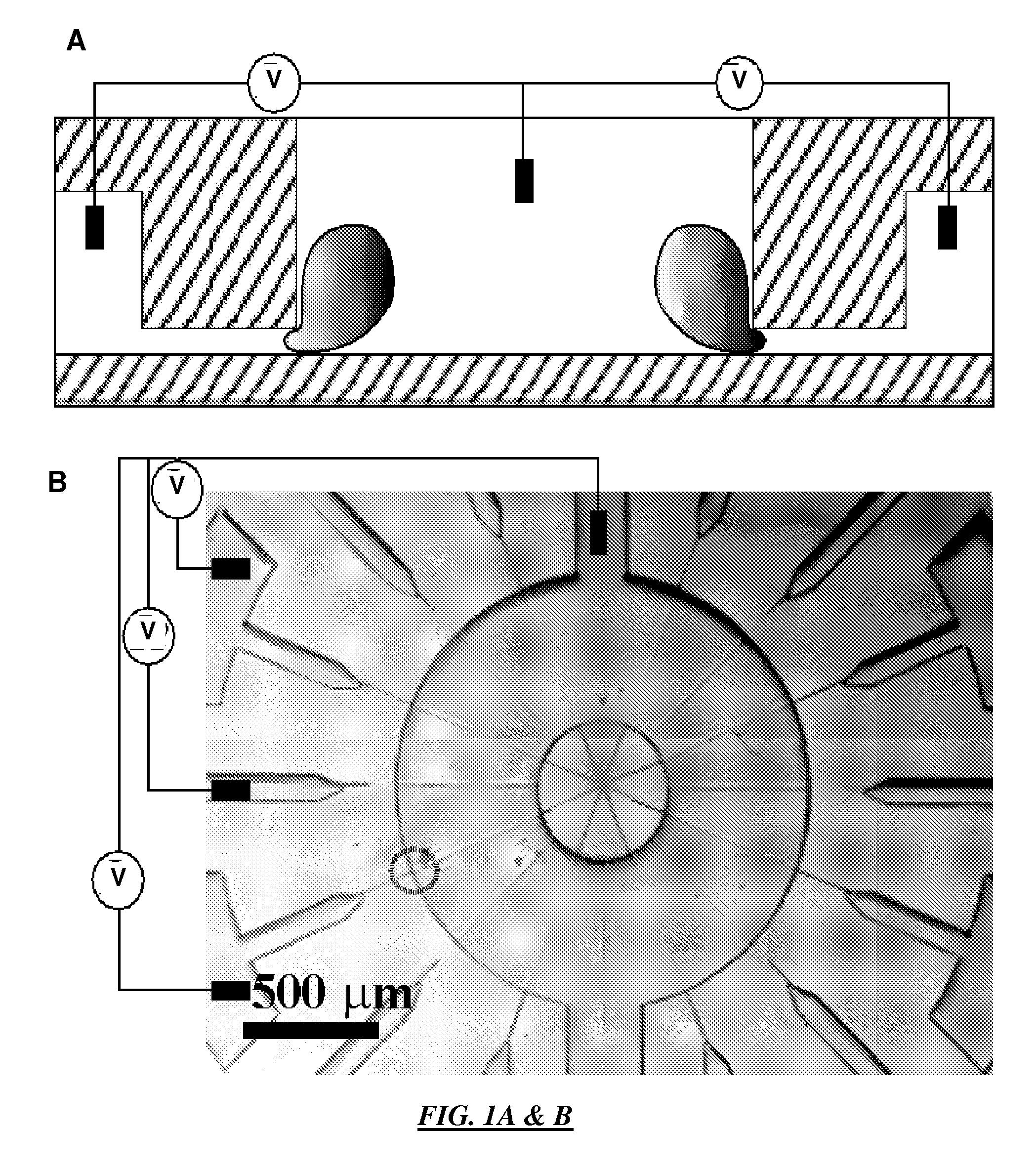
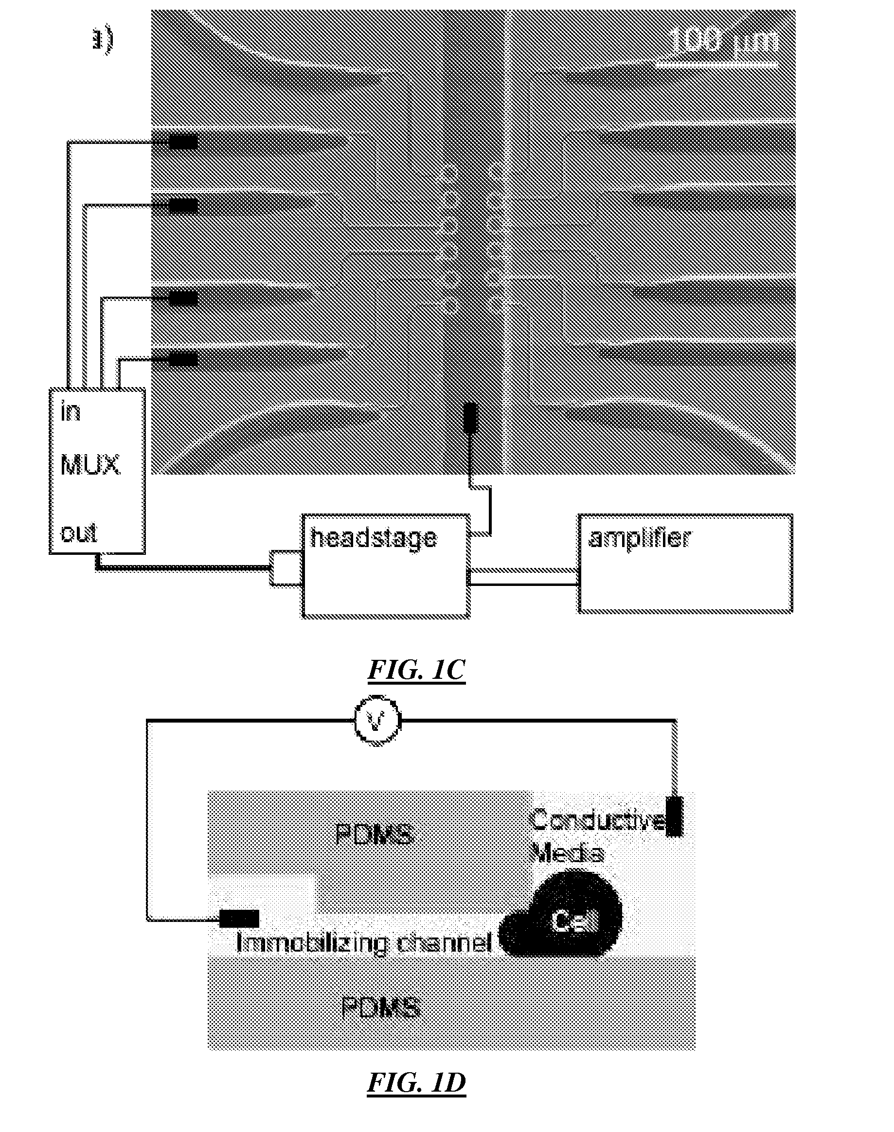
[0096] In an example set-up, Ag / AgCl electrodes are connected via tubing to one of the main channels of the chip, and to one or more of the immobilizing channels. These electrodes, which serve both to apply the voltage and record the current, are good recording electrodes because of their minimal electrical double layer (EDL). The other main channel is connected to a syringe for cell loading. The two electrodes are connected to an amplifier (PC-ONE Patch clamp, Dagan) which provides the voltage and measures the current. The amplifier is controlled by a custom-made Labview (National Instruments) application through a data acquisition card (PCI-6024E, National Instruments). The chip is monitored with an inverted microscope (Eclipse TS100, Nikon) with a fluorescent module and is video captured with a camera (DXC-190, Sony) and a video capture card (microVideo DC50, Pinnacle) on the same computer.

[0097] To start the electroporation experiments, all channels in the chip are filled...

example fabrication

6. Example Fabrication

[0104] Systems and devices as described herein can be fabricated using any techniques or methods familiar from the field of photolithography, nano-fabrication, or micro-fluidic fabrication. For completeness of this disclosure and to discuss additional and independent novel aspects according to specific embodiments of the invention, specifics of example fabrication methods are provided below.

[0105] Example fabrication steps according to specific embodiments of the invention are shown diagrammatically in FIG. 13(a-f). In this example, a silicon or other suitable substrate mold is prepared using surface micromachining and / or photolithography techniques. In other examples, any other appropriate material and any other techniques for making a mold could be used.

[0106] In a micromachining example according to specific embodiments of the invention, first, 3.1 μm height patterns are made, defining the narrow cell trapping channels using deep reactive ion etching (FIG....

example alternative

Fabrication Methods

[0111] The following further example fabrication methods are provided for completeness of this disclosure. It will be recognized from these teachings that many alterations can be made to this method to accommodate different materials and / or methods of manufacturing and / or to provide different configurations as otherwise described herein.

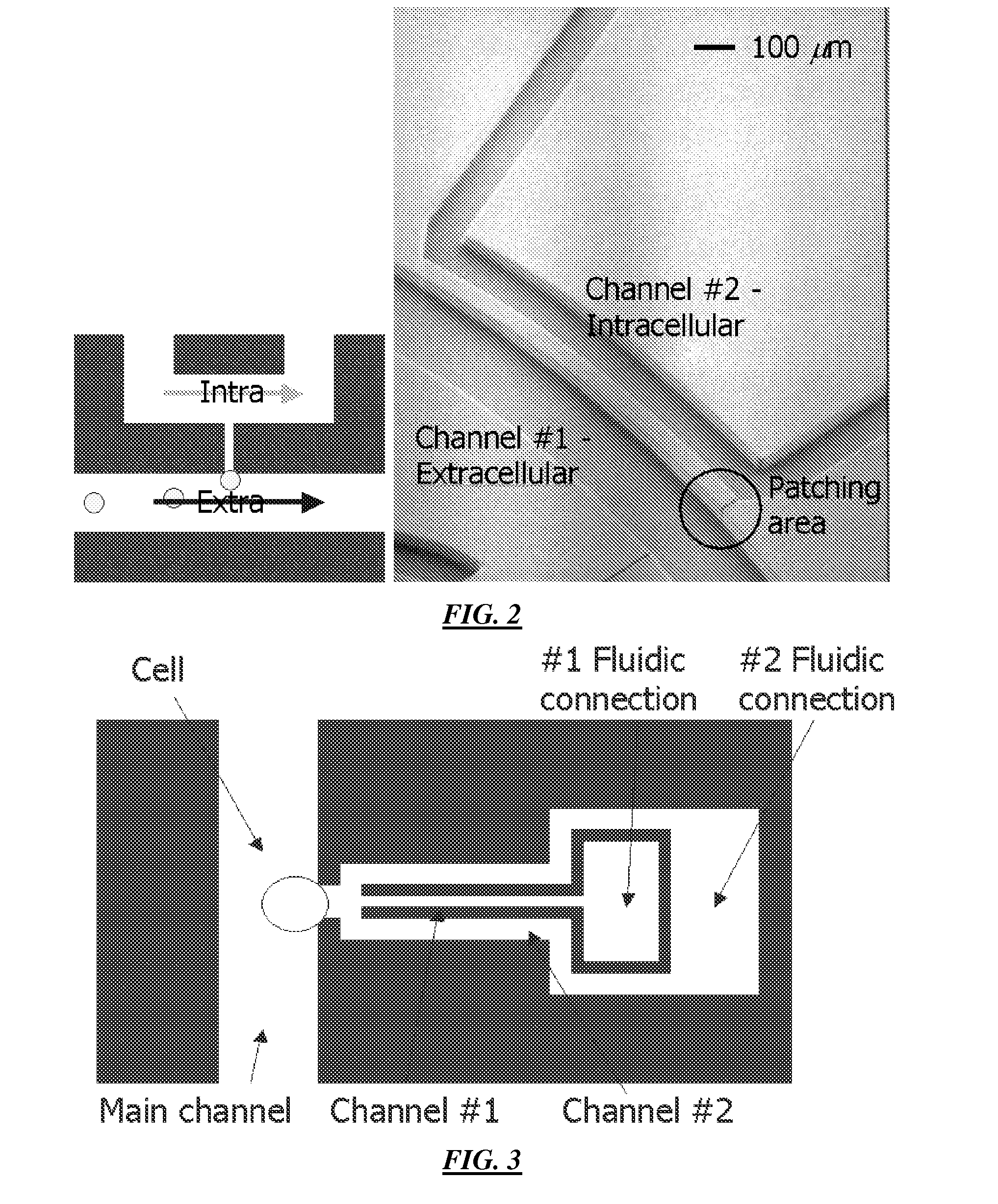
[0112] A specific example device according to embodiments of the invention can be fabricated as follows, similarly as described above. First, a mold is prepared using surface micromachining techniques. As an example, first the narrow patch capillaries are made with 3.1 micron high patterns using deep reactive ion etching. Recording capillaries are 20 microns apart, which allows trapping of, for example, 12 cells along a main channel in a volume of 0.36 nL (150×60×40 micron3 for length, width, and height, respectively). Therefore, in the active device area, the reagent dead volume is 30 pL per recording site. Second, 50 micron high...


PUM

PropertyMeasurementUnit
distanceaaaaaaaaaa
distanceaaaaaaaaaa
voltagesaaaaaaaaaa

Abstract

Method and systems provide improved cell handling in microfluidic systems and devices using lateral cell trapping and methods of fabrication of the same that allow for selective low voltage electroporation and electrofusion.

Description

CROSS REFERENCE TO RELATED APPLICATIONS [0001] This application claims priority from provisional patent application 60 / 710,305 filed 21 Aug. 2005 and is a continuation in part of PCT / US 2005 / 008349, filed 14 Mar. 2005, which claims priority from provisional patent application 60 / 552,892, filed 12 Mar. 2004, all incorporated herein by reference for all purposes.COPYRIGHT NOTICE [0002] Pursuant to 37 C.F.R. 1.71(e), applicants note that a portion of this disclosure contains material that is subject to copyright protection (such as, but not limited to, diagrams, device photographs, or any other aspects of this submission for which copyright protection is or may be available in any jurisdiction.). The copyright owner has no objection to the facsimile reproduction by anyone of the patent document or patent disclosure, as it appears in the Patent and Trademark Office patent file or records, but otherwise reserves all copyright rights whatsoever. FIELD OF THE INVENTION [0003] The present i...

Claims


Application Information

Patent Timeline
Patent Type & Authority Applications(United States)
IPC IPC(8): C12N15/74C12M1/42C12N15/87
CPCB01L3/502707B01L3/502761B01L2200/0668G01N33/48728C12M23/16C12M35/02C12N15/87B01L2400/0487
Inventor LEE, LUKE P.SEO, JEONGGIIONESCU-ZANETTI, CRISTIANKHINE, MICHELLELAU, ADRIAN
Owner RGT UNIV OF CALIFORNIA
Why Eureka
Try Eureka