Methods of manufacturing a three-dimensional semiconductor device and semiconductor devices fabricated thereby

a three-dimensional semiconductor and semiconductor technology, applied in the field of three-dimensional semiconductor structures and methods of forming three-dimensional semiconductor devices, can solve the problems of reducing the electrical characteristics of tft, limiting the size of discrete devices, and affecting the efficiency of the semiconductor devi

Inactive Publication Date: 2007-07-12
SAMSUNG ELECTRONICS CO LTD
View PDF12 Cites 177 Cited by
  • Summary
  • Abstract
  • Description
  • Claims
  • Application Information

AI Technical Summary

Benefits of technology

[0012] Embodiments of the invention provide a method for fabricating three-dimensional semiconductor devices using a single bonding process and a single dela

Problems solved by technology

Unfortunately, limits on the photolithography process, such as the wavelength of the light used, cause there to be limits on the size of the discrete devices.
Consequently, the photolithography process seems to place a limit on the density of semi-conductor devices that can be achieved.
However, large grains in the polysilicon material can act as a carrier trap, thereby degrading the electrical characteristics of the TFT.
As a result, the electrical characteristics of the resulting TFT are not as desirable as that of th

Method used


Image

  • Methods of manufacturing a three-dimensional semiconductor device and semiconductor devices fabricated thereby
  • Methods of manufacturing a three-dimensional semiconductor device and semiconductor devices fabricated thereby
  • Methods of manufacturing a three-dimensional semiconductor device and semiconductor devices fabricated thereby

Examples


Embodiment Construction

[0019] The invention will now be described more fully with reference to the accompanying drawings, in which exemplary embodiments are shown. The invention may, however, be embodied in many different forms and should not be construed as being limited to the embodiments set forth herein; rather, these embodiments are provided so that this disclosure is thorough and complete, and conveys the inventive principles found in embodiments of the invention to those skilled in the art.

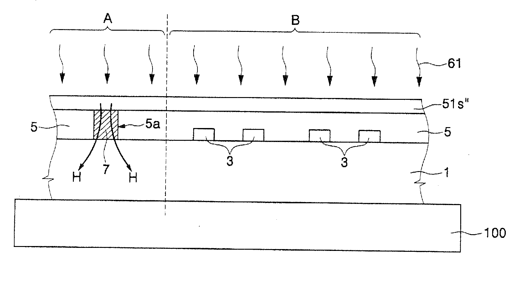
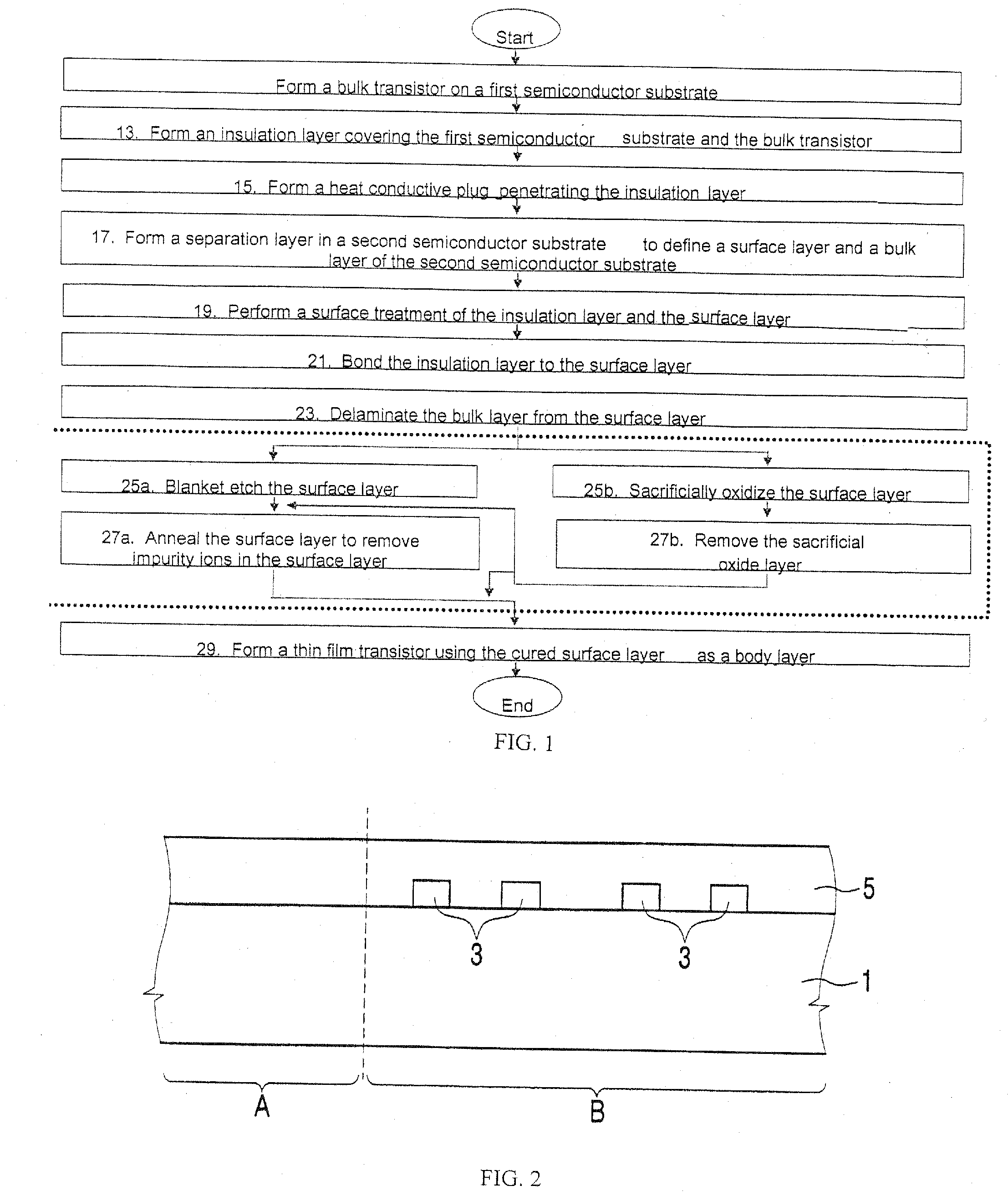
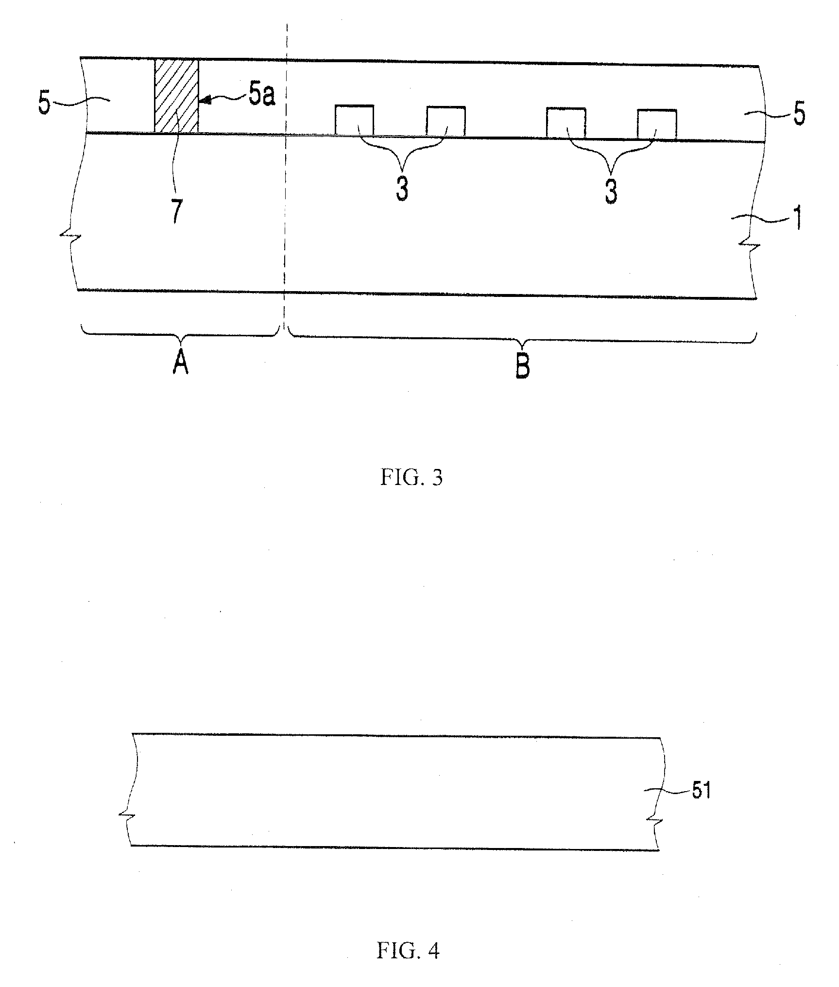
[0020]FIG. 1 is a process flow chart illustrating a method of fabricating a semiconductor device according to some embodiments. FIG. 2 is a cross-sectional view of a first semiconductor substrate according to some embodiments.

[0021] Referring to FIGS. 1 and 2, lower discrete devices or lower devices 3, such as bulk transistors, are formed on the first semiconductor substrate 1. The bulk transistor may refer to a device built on a single-crystal bulk substrate. The first semiconductor substrate 1 may be a silico...


PUM


Abstract

A method of fabricating a three-dimensional semiconductor device is provided along with a three-dimensional semiconductor device fabricated thereby. The method includes forming a heat conductive plug to channel heat away from devices on a substrate, while high temperature processes are performed on a stacked semiconductor layer. The ability to use high temperature processes on the stacked semiconductor layer without adversely effecting devices on the substrate allows the formation of a high quality single-crystalline stacked semiconductor layer. The high quality single-crystalline semiconductor layer can then be used to fabricate improved thin film transistors.

Description

[0001] This application claims priority from Korean Patent Application No. 2006-02839, filed on Jan. 10, 2006, which is herein incorporated by reference in its entirety. BACKGROUND [0002] 1. Technical Field [0003] This disclosure generally relates to the field of semiconductor devices. Specifically, the disclosure relates to three-dimensional semiconductor structures and methods of forming three-dimensional semiconductor devices. [0004] 2. Description of the Related Art [0005] Semiconductor devices, such as semiconductor memories, are in widespread use in consumer electronics and other applications. Consumer demand for ever higher densities of semiconductor devices has motivated manufacturers to seek methods of decreasing the size of discrete devices that typically make up a semiconductor device. The discrete devices include transistors, capacitors and resistors. The discrete devices may be fabricated using various processes such as photolithography, wet and dry etching, thin film d...

Claims


Application Information

Patent Timeline
IPC IPC(8): H01L23/34H01L21/00
CPCH01L21/84H01L21/76254A45D34/045A45D40/18A45D40/265A45D2034/002A46B3/005A46B2200/1053A46B2200/106H01L23/34
Inventor CHA, YONG-WONSUH, DONG-CHULBAE, DAE-LOK
Owner SAMSUNG ELECTRONICS CO LTD
Why Eureka
Try Eureka