Optical thin film with high hardness made by insert mold technology and manufacturing processes thereof

Active Publication Date: 2007-07-12
ENTIRE TECH CO LTD
View PDF0 Cites 25 Cited by
  • Summary
  • Abstract
  • Description
  • Claims
  • Application Information

AI Technical Summary

Benefits of technology

[0013]Therefore, the present invention provides an optical thin film with high hardness made by insert mold technology and manufacturing processes thereof. A hardened layer is formed above the optical thin film that is not hardened. Then a figurative or colored layer is printed under the optical thin film. Later a plastic material is injected under the figurative or colored layer by injection molding. At last, the hardened layer is treated by UV light. Thus there are no problems of cracks, wrinkles and fogging during hot sta

Problems solved by technology

Thus during hot stamping or thermal vacuum processes for shaping the optical thin film, the optical thin f

Method used


Image

  • Optical thin film with high hardness made by insert mold technology and manufacturing processes thereof
  • Optical thin film with high hardness made by insert mold technology and manufacturing processes thereof
  • Optical thin film with high hardness made by insert mold technology and manufacturing processes thereof

Examples


Example

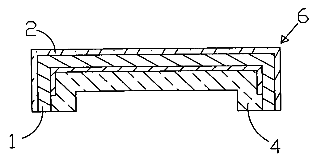
[0025]During a conventional IMD technology, while taking the steps of hot stamping or thermal vacuum forming, the optical thin film has been through hardening treatment so there may be problems of cracks, wrinkles or fogging. Thus the present invention provides an optical thin film with high hardness made by insert mold technology and manufacturing processes thereof for improving above disadvantages.

[0026]Refer from FIG. 3 to FIG. 3D, in step S200, prepare an optical thin film 1 that has not been through hardening treatment. The material of the optical thin film 1 is selected from one of the followings: polyethylene terephthalate (PET), polycarbonate (PC), Triacetyl Cellulose (TAC), polymeric methyl methacrylate (PMMA), methyl methacrylate styrene copolymer (MS), and cyclic olefins copolymer (COC). In this embodiment, take film made from polycarbonate as an example, the thickness of the film is 250 μm while the grade of hardness is 2 B.

[0027]Refer to step S210, a hardened layer is f...


PUM

PropertyMeasurementUnit
Thicknessaaaaaaaaaa
Thicknessaaaaaaaaaa
Thicknessaaaaaaaaaa

Abstract

An optical thin film with high hardness made by insert mold technology and manufacturing processes thereof are disclosed. The optical thin film is applied on surface of a plastic housing for increasing hardness of the plastic housing so as to prevent scratches. During manufacturing processes of insert mold for producing a hard coating film, the step of hardening treatment is moved to the last step so as to avoid cracks on the optical thin film generated during the procedures. Thus the yield rate is increased and the manufacturing cost is reduced.

Description

BACKGROUND OF THE INVENTION[0001]The present invention relates to a plastic film, especially to an optical thin film made by insert mold technology and manufacturing processes thereof.[0002]Due to prevalence of mobile phones and notebooks, users have higher demands of housings of them. Besides requirements of styles and colors, hardened surface for preventing scratches is also important. The hardening treatment for preventing scratches is applied on electronics such as notebooks, mobile phones, and personal digital assistants (PDA) with colorful and smooth plastic surface made by injection molding. Besides, it can also be applied to wood panels and wheel rims.[0003]Refer to FIG. 1, a conventional way for surface coating of a film on plastic housings is disclosed. Refer to step S100′, prepare a plastic material made from polycarbonate (PC), polypropylene (PP), polymeric methyl methacrylate (PMMA), methyl methacrylate styrene copolymer (MS), acrylonitrile butadine styrene (ABS), polys...

Claims


Application Information

Patent Timeline
IPC IPC(8): G11B5/64B32B17/10
CPCB29C45/0053B29C45/1418B29C45/14688B29C45/14811Y10T428/31B29C2045/14877B29K2995/002B29K2995/0087Y10T428/265B29C2045/0075
Inventor HSIEH, SHAN-ERWANG, JYI-HORNGCHANG, JEN-HUAI
Owner ENTIRE TECH CO LTD
Why Eureka
Try Eureka