Ferroelectric capacitor and method for fabricating the same

Inactive Publication Date: 2007-07-12
PANASONIC CORP
View PDF3 Cites 3 Cited by
  • Summary
  • Abstract
  • Description
  • Claims
  • Application Information

AI Technical Summary

Benefits of technology

[0015]As shown above, the present invention can offer the ferroelectric capacitor which prevents degradation of ferroelectric materials during a semiconductor fabrication process, particularly a decrease in electric

Problems solved by technology

In the first conventional example, since the Curie temperature Tc of the ferroelectric is lowered, the capacitor operates unstably at high temperatures.
This in turn degrades the characteristics of retention or imprint reliabi

Method used


Image

  • Ferroelectric capacitor and method for fabricating the same
  • Ferroelectric capacitor and method for fabricating the same
  • Ferroelectric capacitor and method for fabricating the same

Examples


Example

First Embodiment

[0027]A ferroelectric capacitor and its fabrication method according to a first embodiment of the present invention will be described.

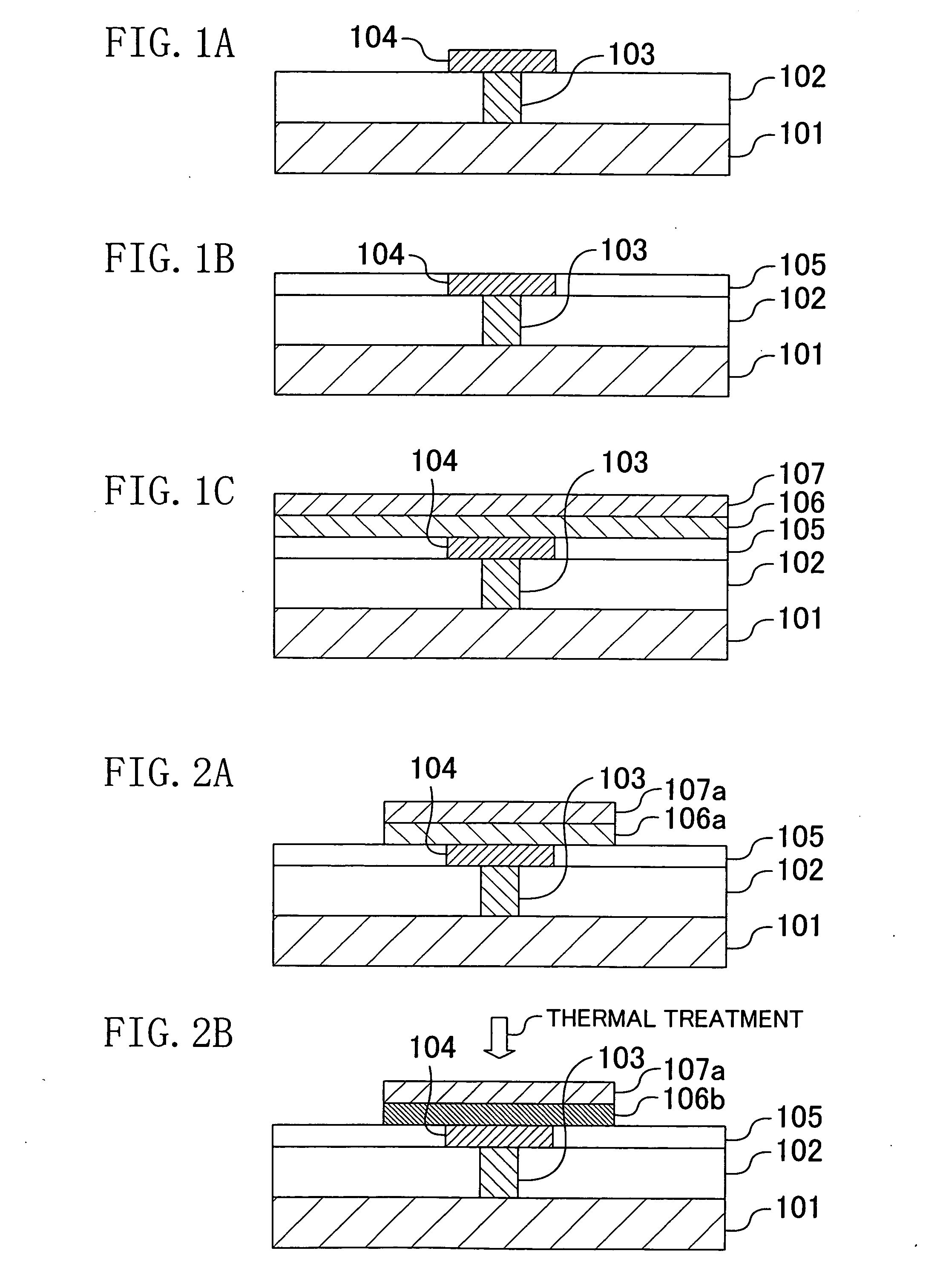
[0028]FIGS. 1A to 1C and 2A and 2B are sectional views showing a method for fabricating a ferroelectric capacitor according to the first embodiment of the present invention in the order of its fabrication process steps.

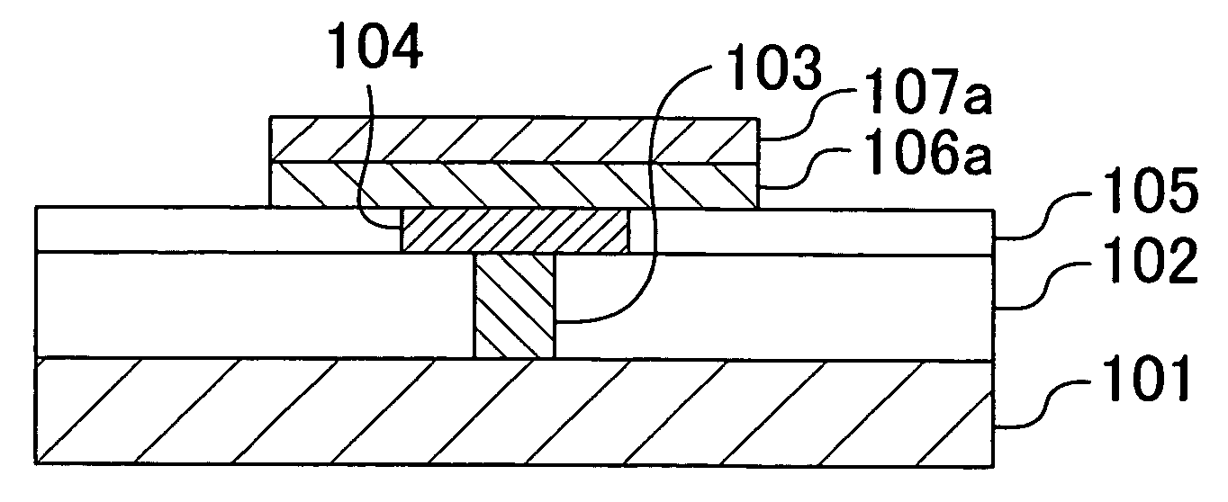
[0029]Referring to FIG. 1A, on a semiconductor substrate 101 with memory cell transistors (not shown) and the like formed thereon, a first interlayer insulating film 102 is formed which is made of, for example, a BPSG (SiO2 with B, P, and the like added therein) film. Subsequently, the first interlayer insulating film 102 is formed with a contact plug 103 of tungsten, polysilicon, or the like whose bottom end reaches the top surface of the semiconductor substrate 101. Then, a lower electrode 104 made by sequentially stacking a barrier layer and a noble metal layer in this order is formed on the first interlayer insulatin...

Example

Second Embodiment

[0052]A second embodiment of the present invention will describe a fabrication method of a ferroelectric capacitor capable of providing an excellent percentage of polarization reversal relative to the thickness of a ferroelectric film as described above in the first embodiment. In the second embodiment, the description is divided according to materials constituting the ferroelectric film.

—Ferroelectric Film Made of SBTN—

[0053]FIGS. 5A to 5C and 6A and 6B are sectional views showing a fabrication method of a ferroelectric capacitor made of SBTN according to the second embodiment of the present invention in the order of its fabrication process steps.

[0054]Referring to FIG. 5A, on a semiconductor substrate 201 with memory cell transistors (not shown) and the like formed thereon, a first interlayer insulating film 202 is formed which is made of, for example, a BPSG (SiO2 with B, P, and the like added therein) film. Subsequently, the first interlayer insulating film 202 ...


PUM

PropertyMeasurementUnit
Fractionaaaaaaaaaa
Timeaaaaaaaaaa
Timeaaaaaaaaaa

Abstract

In a ferroelectric capacitor comprising: a lower electrode; a ferroelectric film formed on the lower electrode; and an upper electrode formed on the ferroelectric film, the coercive voltage of the ferroelectric film is 1.5 V or less and the polarization switching time of the ferroelectric film is 200 ns or less.

Description

BACKGROUND OF THE INVENTION[0001](a) Fields of the Inventions[0002]The present invention relates to ferroelectric memory devices using dielectric materials, and to ferroelectric capacitors and their fabrication methods capable of enhancing the speed at which the polarization of a ferroelectric film is reversed.[0003](b) Description of Related Art[0004]In the development of ferroelectric memory devices, in order to fabricate the devices having stack structures with a large capacity of 256 kbit to 4 Mbit, a significant increase in degree of integration of the devices, that is, miniaturization of the devices is indispensable. Moreover, the devices are required to operate at high speed.[0005]For example, a first conventional example (see, for example, Japanese Laid-open Patent Publication No. H7-99252) proposes the high-speed operation method as described below. In the case where a ferroelectric film made of PZT(PbZrxTi1−xO3) with a ferroelectric crystal structure of ABO3 (where A and B...

Claims


Application Information

Patent Timeline
IPC IPC(8): H01L21/00
CPCH01G4/085H01G4/1254H01L28/65H01L28/55H01G4/33
Inventor HAYASHI, SHINICHIRONASU, TORU
Owner PANASONIC CORP
Why Eureka
Try Eureka