Organic electroluminescent element and the manufacturing method

a technology of electroluminescent elements and manufacturing methods, applied in the direction of discharge tubes/lamp details, discharge tubes luminescnet screens, electric discharge lamps, etc., can solve the problems of film defects that cannot be suppressed, quality deterioration, and film defects that cannot be hidden

Inactive Publication Date: 2007-07-19
TOPPAN PRINTING CO LTD
View PDF9 Cites 37 Cited by
  • Summary
  • Abstract
  • Description
  • Claims
  • Application Information

AI Technical Summary

Problems solved by technology

As for the organic electroluminescent element, quality deteriorates due to influence of atmospheric water vapor and oxygen.
Film defects such as a cavity and a pinhole of a film inside or a crack of a film occur due to a projection of an electrode and a substrate, and a particle.
Then even if a film is thickened, and another film is laminated on the film formed beforehand, film defects cannot be suppressed.
Cleaning of an organic resin film formation chamber is difficult.
Therefore, there is a problem in mass production.
In addition, in this method, a defect remains in each inorganic film.
Therefore, if the number of layers of laminated films is less than about 5 or 6, barrier property of an organic electroluminescent element is not sufficient.
However, in technique with the use of this counterbored glass, thin organic electroluminescent element cannot be made.
However, water vapor permeability of an adhesive itself is high.
Therefore, this sealing method is inferior to a conventional sealing method using a cap.
However, it has not resulted in fundamental solution.
However, an organic electroluminescent element deteriorates when sealing ability of a barrier film is not sufficient.
In other words this barrier film is a barrier film which is insufficient for a protective layer of an organic electroluminescent element.
Therefore, the conventionally proposed protective layer of an organic electroluminescent element with the use of a flat glass is insufficient for a seal of an organic electroluminescent element.

Method used


Image

  • Organic electroluminescent element and the manufacturing method
  • Organic electroluminescent element and the manufacturing method
  • Organic electroluminescent element and the manufacturing method

Examples


first embodiment

Barrier film (The First Embodiment)

[0102]The following barrier film can be used: Metallic oxide such as silicon dioxide or aluminium oxide; Metal fluoride such as aluminum fluoride or magnesium fluoride; Metal nitrides such as silicon nitride or aluminum nitride; Metal oxynitride such as silicon oxide nitride; and Metal carbide such as silicon carbide.

[0103]Especially it is preferable to use silicon nitride, silicon dioxide and silicon oxynitride which are superior in barrier properties. Especially silicon nitride is preferable from the viewpoint of barrier property.

[0104]In addition, as for silicon nitride, silicon dioxide and silicon oxynitride, depending on the kind of a film formation method, hydrogen and carbon may be included in a film. However, these barrier films can be used if necessary.

[0105]According to a material of a barrier film, the following formation method of a barrier film can be used: Resistance heating evaporation method, electron-beam evaporation method, reacti...

second embodiment

Barrier Film (The Second Embodiment)

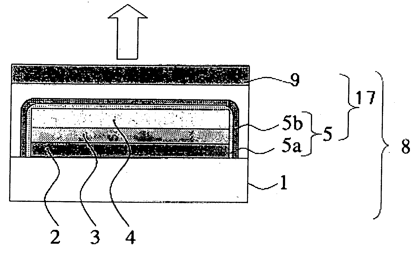
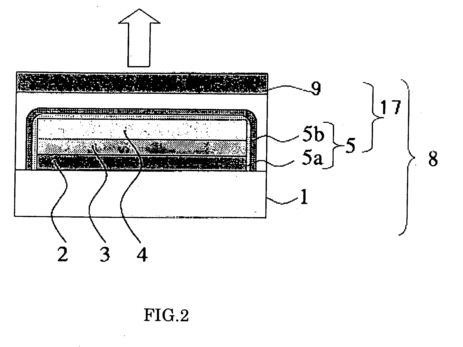
[0128]For barrier film 5, easily oxidative silicon nitride film 5b and water-vapor-proofing silicon nitride film 5a are used. Balancing high barrier property and transparency is possible by using a silicon nitride film as a main film of barrier film 5. Therefore, light can be taken out from sealing substrate 9 side.

[0129]In addition, sputtering, photo-assisted CVD and plasma enhanced CVD can be used for film production technique.

[0130]Plasma enhanced CVD is the most desirable in this application. In plasma enhanced CVD technique, all the reaction generating film-forming seed takes place in gas phase. Therefore, it is not necessary for a reaction to be caused in a substrate surface. Therefore, plasma enhanced CVD is most suitable for low temperature film forming method needed in this application. Besides, a thin film can be formed in various conditions by controlling a gaseous flow rate, temperature of a substrate, gas pressure in a film production...

example 1

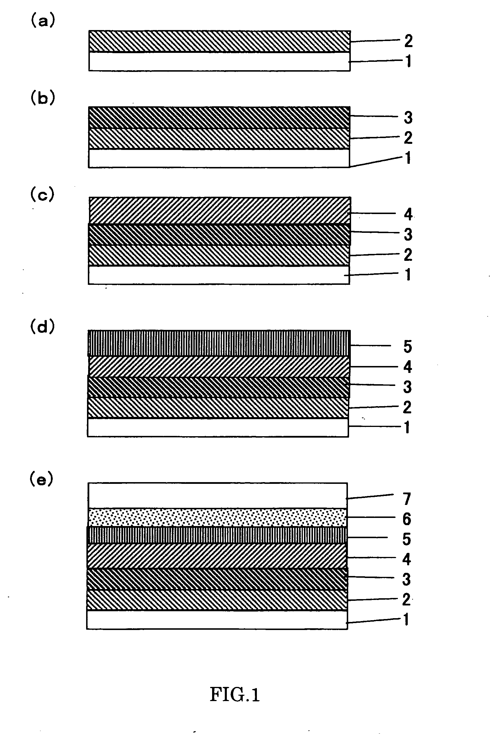
[0152]Glass was used for substrate 1. The ITO film of which thickness was 150 nm was formed on substrate 1 as a first electrode by a sputtering method. Patterning of ITO film was performed using photo-lithography etching method.

[0153]Organic luminescent medium layer 3 was made next. A mixture of poly (3,4-ethylenedioxy thiophen) and polystyrene sulfonate was used as a hole transport layer (thickness: 20 nm). Poly [2-methoxy-5-(2′-ethyl-hexyloxy)-1,4-phenylenevinylene] (MEHPPV) was used as an organic luminescent layer(thickness: 100 nm). Each layer was formed by a spin coat method.

[0154]As a second electrode, Ca film (5 nm) and Al film (100 nm) were formed by evaporation method next.

[0155]Barrier film was layered using plasma enhanced CVD technique next. After having layered a low density silicon nitride film (2.3 g / cm3) of which thickness was 200 nm, a normal density barrier film (2.8 g / cm3) of which thickness was 200 nm was layered.

[0156]The obtained organic electroluminescent elem...


PUM


Abstract

One embodiment of an organic electroluminescent element of present invention includes a substrate, a first electrode on the substrate, an organic luminescent medium layer including an organic luminescent layer on the first electrode, a second electrode on the organic luminescent medium layer and barrier film formed on the second electrode. The organic luminescent medium layer is sandwiched between the first electrode and the second electrode. Film density of the barrier film changes in thickness direction.

Description

CROSS REFERENCE[0001]This application claims priority to Japanese application number 2006-10739, filed on Jan. 19, 2006, and priority to Japanese application number 2006-116527, filed on Apr. 20, 2006, which are incorporated herein by reference.BACKGROUND OF THE INVENTION[0002]1. Field of the Invention[0003]The present invention is related to an organic electroluminescent element. It is expected that an organic electroluminescent element is used for wide variety of applications. Applications of an organic electroluminescent element include a flat panel display used in a television, a PC monitor, portable units such as a portable telephone, a surface emitting light source, an illumination, and a light emission type advertisement body.[0004]2. Description of the Related Art[0005]Because an organic electroluminescent element has the following merit, an organic electroluminescent element is expected as a flat panel display as a substitute for a CRT and a liquid crystal display.[0006]1. ...

Claims


Application Information

Patent Timeline
Patent Type & Authority Applications(United States)
IPC IPC(8): H01L51/00
CPCH01L51/5237H10K50/841H10K50/844
Inventor OOSONO, TETSUONAKAMURA, AKIOKOMORI, TSUNENORI
Owner TOPPAN PRINTING CO LTD
Why Eureka
Try Eureka