Nano-contacted magnetic memory device

a magnetic memory and non-contact technology, applied in the field of magnetic memory devices, can solve the problems of non-uniform cell resistance generation errors, key problems of fatigue properties, and non-uniform cell resistance, and achieve the effect of low cost and high density

Inactive Publication Date: 2007-07-19
AGENCY FOR SCI TECH & RES
View PDF11 Cites 49 Cited by
  • Summary
  • Abstract
  • Description
  • Claims
  • Application Information

AI Technical Summary

Benefits of technology

[0009] In a first embodiment of the present invention, a high density and low cost MRAM unit is presented. The MRAM unit includes a substrate, a plurality of transistors formed on said substrate, a common memory block, a plurality of contacts, and a common electrode. Each of the plurality of transistors is a field-effect transistor including a first source / drain electrode, a second source / drain electrode and a gate electrode. The common memory block includes a ferromagnetic recording layer, a free magnetic reading layer, a non-magnetic space layer between the ferromagnetic recording layer and the free magnetic reading layer, and a plurality of active areas defined in the common memory block. Each of the plurality of contacts electrically connects a respective one of the first source / drain electrodes with a corresponding one of the plurality of active areas. The common electrode is in electrical contact with the plurality of contacts through the common memory block and serves as bit line for the first source / drain electrodes. Each of the plurality of active areas forms an effective magnetoresistive element. Each of the plurality of transistors is controllable to electrically activate a corresponding one of the plurality of contacts and thereby to write / read a data bit into / from the ferromagnetic recording layer at a respective one of the effective magnetoresistive elements.

Problems solved by technology

However, the fatigue property is a key issue in CRAM due to high temperature heating.
The cell uniformity in products is also a key issue due to the reading method.
Since the cell resistance is detected during reading, any non-uniform cell resistance generates an error.
As mentioned above, the uniformity of the resistance of the CPP spin-valve element is a key issue.

Method used


Image

  • Nano-contacted magnetic memory device
  • Nano-contacted magnetic memory device
  • Nano-contacted magnetic memory device

Examples


Embodiment Construction

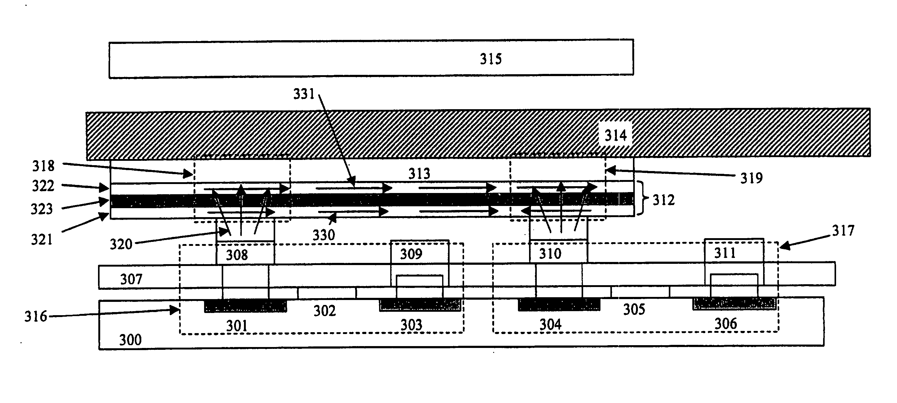
[0028] It is pointed out that in the present application the term “critical temperature” is substantially the blocking temperature for antiferromagnetic (AFM) material, which can be less than the Néel temperature. The critical temperature is substantially the Curie temperature for ferromagnetic material. The blocking temperature of an AFM layer is the temperature at or above which the AFM layer loses its ability to “pin” (i.e. fix) the magnetization of an adjacent ferromagnetic layer below the Curie temperature of the adjacent ferromagnetic layer.

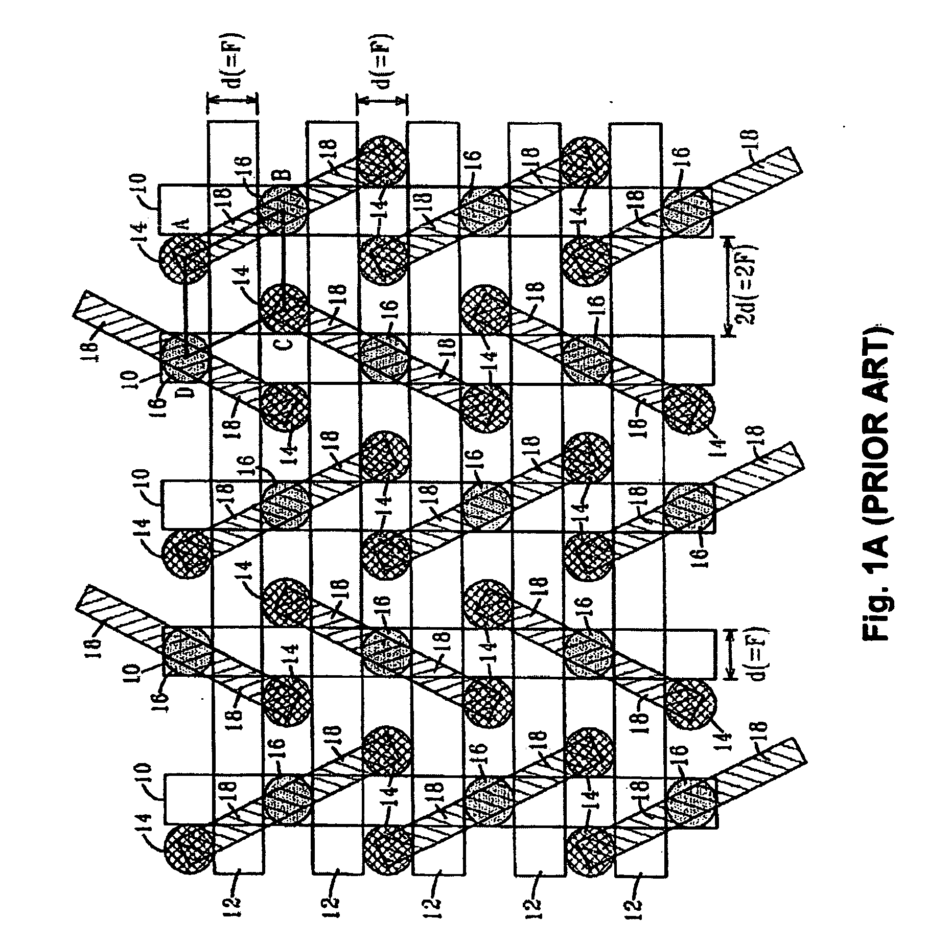
[0029]FIG. 1A shows a top view of a layout of a 6F2 DRAM cell structure according to the prior art. The DRAM cell structure includes vertical bit lines 10, horizontal word lines 12, capacitor contacts 14, bit line contacts 16, and active (diffusion) areas 18 that include each a source region and a drain region. The word lines 12 electrically contact with gate electrodes (not shown) and the bit lines 10 electrically contact with the source ...


PUM


Abstract

A magnetic memory device includes a plurality of transistors (316, 317) formed on a substrate and a common magnetic memory block (312) including multiple effective magnetoresistive elements (318, 319), a ferromagnetic recording (321), a non-magnetic space (323), and a free magnetic reading (322) layer formed above the transistors (316, 317). An extended common digital line (315) is located above the common magnetic memory block (312). The common magnetic memory block (312) is electrically connected with a respective source/drain electrode of the transistors (316, 317) through each a contact at a respective active area. The specific magnetization state of the ferromagnetic recording layer at the active areas can be changed by a heating process and applying an external field induced from the common digital line (315) and the bit (309, 311) or word (307) or word (307) lines. The change in resistance of the effective magnetoresistive element (318, 319) can be detected by means of changing the magnetization state of the free magnetic reacting layer during reading, thus a smaller switching field is required.

Description

FIELD OF THE INVENTION [0001] The present invention relates to a magnetic memory device. In particular, it relates to a magnetoresistive random access memory (MRAM) device with current-perpendicular-to-plane (CPP) MRAM cells that write data by thermal assisted techniques. BACKGROUND OF THE INVENTION [0002] Memory devices are used in a wide variety of applications. Such applications include personal computers, consumer products such as digital cameras, digital video cameras and mobile phones. There exist many different memory devices. The type of memory devices chosen for a specific function depends largely upon what features of these devices are best suited to perform that specific function. For instance, volatile memories, such as dynamic random access memories (DRAMs) must be continually powered in order to retain their contents. However, DRAMs tend to provide greater storage capability and programming option and cycle than non-volatile memories such as read only memories (ROMs). ...

Claims


Application Information

Patent Timeline
Patent Type & Authority Applications(United States)
IPC IPC(8): G11C11/00G11C11/15G11C11/16
CPCG11C11/16H01L43/08H01L27/228H10B61/22H10N50/10
Inventor ZHENG, YUANKAIWU, YIHONG
Owner AGENCY FOR SCI TECH & RES
Why Eureka
Try Eureka