Precursor Containing Copper Indium And Gallium For Selenide (Sulfide) Compound Formation

a technology of selenide and compound, which is applied in the field of precursors containing copper indium and gallium for selenide (sulfide) compound formation, can solve the problems of compound film peeling, poor adhesion of cuinsesub>2 /sub>film to the mo contact layer, and high cost of electricity generated by silicon-based solar cells, so as to achieve the effect of efficient use of expensive materials

Inactive Publication Date: 2007-07-19
SOLOPOWER
View PDF13 Cites 47 Cited by
  • Summary
  • Abstract
  • Description
  • Claims
  • Application Information

AI Technical Summary

Benefits of technology

[0014] In one aspect, there is provided a method of efficiently u

Problems solved by technology

However, the cost of electricity generated using silicon-based solar cells is higher than the cost of electricity generated by the more traditional methods.
In practice, however, this technique was found to yield CuInSe2 films with poor adhesion

Method used


Image

  • Precursor Containing Copper Indium And Gallium For Selenide (Sulfide) Compound Formation
  • Precursor Containing Copper Indium And Gallium For Selenide (Sulfide) Compound Formation
  • Precursor Containing Copper Indium And Gallium For Selenide (Sulfide) Compound Formation

Examples


example 1

[0027] An acidic indium plating electrolyte was prepared using sulfamate chemistry. The electrolyte contained about 100 grams of indium metal. Sulfumic acid was used to adjust the pH to about 2. A basic Ga plating solution was also prepared using 1 M gallium chloride and adjusting the pH to about 14 using potassium hydroxide. Platinum (Pt) mesh was used as the anode for all depositions.

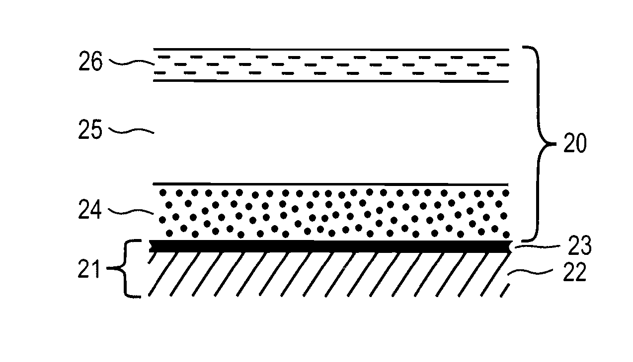
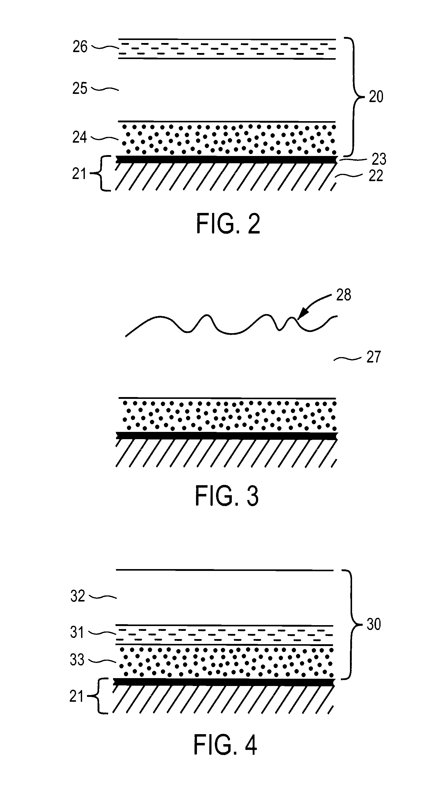
[0028] A glass substrate / Molybdenum (Mo) was used as the base. Mo layer was sputter deposited on the glass surface to a thickness of about 0.7 um. A Cu layer was then deposited by sputtering to a thickness of about 2000 A. Copper deposition by PVD was followed by electro-deposition of a Ga layer from the above solution to a thickness of about 950 A using a current density of about 10 mA / cm2. This was then followed by electro-deposition of In to a thickness of about 3800 A at a current density of about 20 mA / cm2. Gallium electro-deposition efficiency was determined to be at least about 70%, and In ele...

example 2

[0029] The above experiment was repeated, however, this time Cu layer was electro-deposited onto the Mo surface using a copper sulfate electrolyte containing about 150 grams / liter of copper sulfate penta hydrate and about 10 grams / liter of sulfuric acid. It was observed that when Ga electro-deposition was carried out on this electroplated Cu layer, deposition efficiency was much lower (e.g., less than about 30%) and the film was not very continuous.

[0030] The above work demonstrated feasibility of electrodepositing Ga and In on PVD deposited Cu layer so that a precursor stack containing Cu, In and Ga is obtained. Also it is demonstrated that Cu, In and Ga amounts in this stack can be varied at will to obtain the desired Cu / (In+Ga) and Ga / (In+Ga) molar ratios for best solar cell efficiency. To form the compound layer, the precursor stacks of this invention may be reacted with Se and / or S in various ways. One approach is to deposit a Se layer on the precursor stack to form a composit...


PUM


Abstract

The present invention relates to systems and methods for preparing metallic precursor thin films for the growth of semiconductor compounds to be used for radiation detector and solar cell fabrication. In one aspect, there is provided a method of efficiently using expensive materials necessary for the making of solar cells.

Description

CLAIM OF PRIORITY [0001] This application claims priority to U.S. Provisional Application Ser. No. 60 / 756,750 filed Jan. 6, 2007, entitled Precursor Copper Indium And Gallium For Selenide (Sulfide) Compound Formation, and is a continuation-in-part of U.S. application Ser. No. 11 / 081,308 filed Sep. 15, 2005 entitled Technique And Apparatus For Depositing Thin Layers Of Semiconductors For Solar Cell Fabrication, the contents of which applications are incorporated herein by reference in their entirety.BACKGROUND OF THE INVENTION [0002] 1. Field of the Invention [0003] The present invention generally relates to solar cell fabrication. More particularly, the present invention relates to systems and methods for preparing metallic precursor thin films for the growth of semiconductor compounds to be used for radiation detector and solar cell fabrication. [0004] 2. Description of the Related Art [0005] Solar cells are photovoltaic devices that convert sunlight directly into electrical power....

Claims


Application Information

Patent Timeline
IPC IPC(8): H01L21/20
CPCH01L21/02568H01L21/02614Y02E10/541H01L31/0322H01L21/02628
Inventor BASOL, BULENT M.
Owner SOLOPOWER
Why Eureka
Try Eureka