Reset circuit, data carrier and communication device

a technology of data carrier and reset circuit, applied in the field of reset circuit, can solve the problems of incomplete operation, failure to carry out, and remained risky of manipulation

Inactive Publication Date: 2007-07-26
NXP BV
View PDF7 Cites 36 Cited by
  • Summary
  • Abstract
  • Description
  • Claims
  • Application Information

AI Technical Summary

Benefits of technology

[0016] According to the measures claimed in claim 4 the advantage derived is that the data carrier can work as a standalone device. The additional provision of a pad for wired data transfer does not affect the option of constructing a hybrid data carrier.
[0017] According to the measures as claimed in claim 5 the advantage derived is that the data carrier does not need any battery of its own. An optional energy storage means in the form of a coil or a condenser should be designed in such a manner that, in the event of failure of the electromagnetic field, the reset circuit can still continue to work long enough to generate a reset signal and thereby set the data carrier or its logic circuit reliably to a defined logical state.
[0018] According to the measures as claimed in claim 6 the advantage derived is that the data carrier can be used simultaneously for mobile phone applications and for applications relating to wireless data carriers, such as “smart cards” etc. This offers a large range of possible applications e.g. ticket ordering systems, electronic payment systems, secure electronic communication with authorities etc.
[0019] According to the measures as claimed in claim 8 the advantage derived is that the communication device forms a relay station for constructing a virtual smart card system.
[0020] According to the measures as claimed in claims 9 and 10 the advantage derived is that the reset circuit according to the invention remains functional even in those extreme cases where the electromagnetic field of a reader station, that means that the carrier signal is switched off completely and therefore neither clock signals nor data signals are present. At least one of these signals is simulated by the measures according to the invention.
[0021] According to the measures as claimed in claim 11 the advantage derived is that virtual smart card systems can be realized with standard devices.

Problems solved by technology

The known mobile device, however, suffers from a disadvantage that, under certain circumstances in case of a break in the wireless communication between the smart card and the reader station, the operation of the smart card is not terminated properly, but persists in a state which is also called “hang”, in which state it is possible to carry out fraudulent manipulations on the smart card.
While the breaking off of communication for a passive data carrier of a reader station, which carrier is supplied with electrical energy by means of electromagnetic signals, for example a carrier signal, generally remain without any result, because an energy storage (condenser) provided in the data carrier is emptied soon (within a range of milliseconds to seconds) and thus the time period for fraudulent manipulation till the complete switch-off of the data carrier is very short, the risk of manipulation remains on a data carrier that either has its own energy supply in the form of a battery or is installed in a communication device as a “virtual Smart Card” and is supplied with energy from the communication device, till either the battery of the data carrier is exhausted or the communication device is switched off.

Method used


Image

  • Reset circuit, data carrier and communication device
  • Reset circuit, data carrier and communication device
  • Reset circuit, data carrier and communication device

Examples


Embodiment Construction

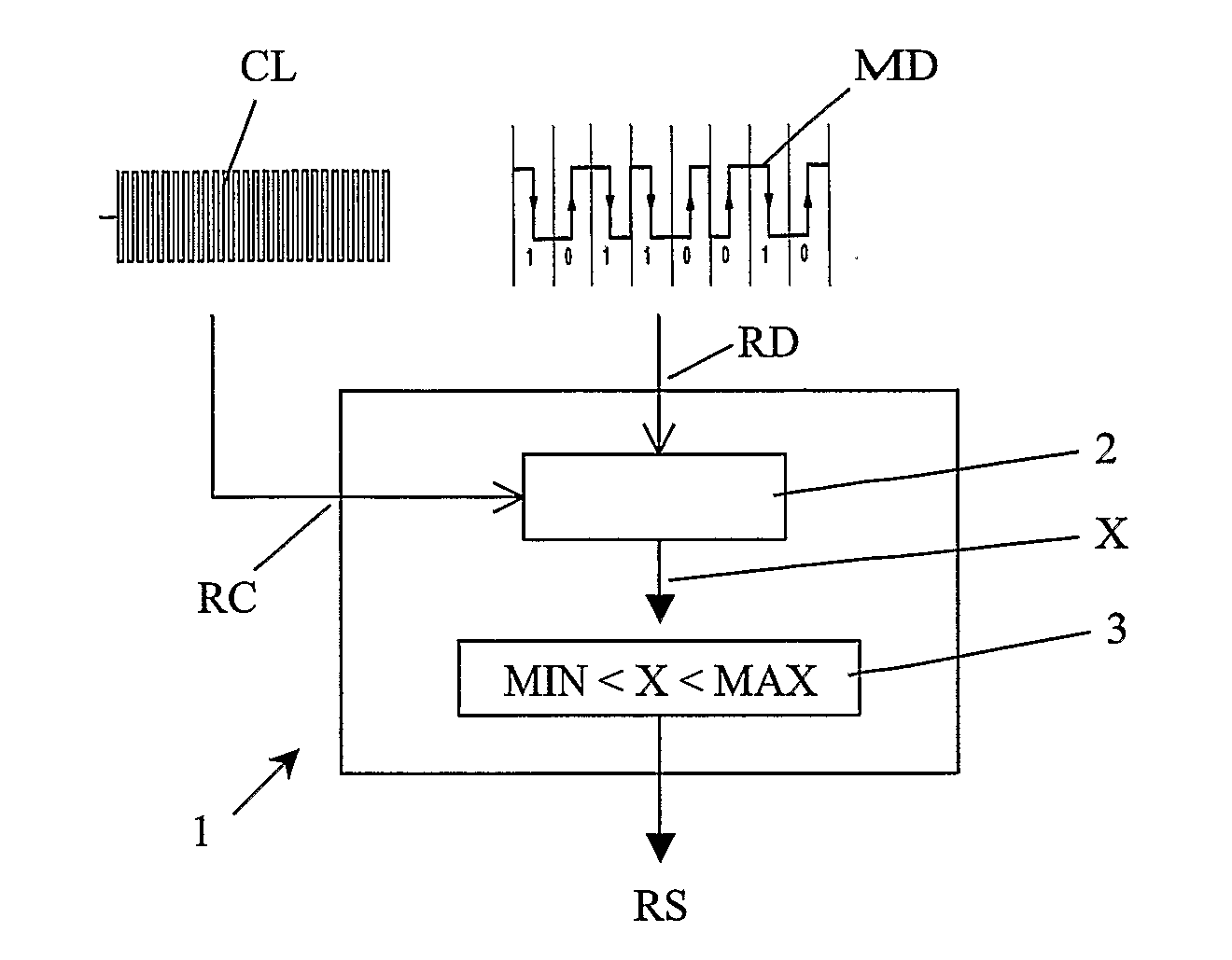
[0027]FIG. 1 shows a reset circuit 1 in form of a block circuit diagram. The reset circuit 1 comprises a clock pulse input RC, by which the reset circuit 1 receives a clock signal CL consisting of a sequence of clock signal cycles. Furthermore, the reset circuit 1 comprises a data signal input RD, by which it receives digital data signals MD. The digital data signals MD are encoded in such a way that they exhibit at least one signal edge (0→1, 1→0) per data bit. In the embodiment depicted, the data signal MD has Manchester coding, so each binary 1 is represented by a negative edge (1→0) in a half-bit period and each binary 0 by a positive edge (0→1) in a half-bit period. Furthermore, the reset circuit 1 comprises a counting stage, called counter 2 for short. Said counter 2 being connected with the data input RD and the clock input RC. The counter 2 is designed for counting a number X of clock pulse cycles, which appear between a defined number of data signal edges. In the simplest c...


PUM


Abstract

In a reset circuit (1) comprising a clock signal input (RC) for receiving a clock singal CL MD signal (CL) consisting of a sequence of clock signal cycles, and comprising a data signal input (RD) for receiving digital data signals (MD), which are encoded in such a manner that at least one signal edge (0→1, 1→ 0) appears per data bit in the data signal, are provided a counter (2) being connected to the data signal input (RD) and the clock signal input (RC) and being designed for counting the number (X) of clock signal cycles, which appear between a defined number of data signal edges, and comparing means (3), which comparing means (3) being designed for comparing the number (X) of clock signal cycles counted by the counter (2) with a lower limit (MIN) and/or with an upper limit (MAX) and which comparing means (3) being designed to produce a reset signal (RS), if the number (X) either remains below the lower object (MIN) or exceeds the upper limit (MAX), depending on the limit value (MIN, MAX) taken for comparison.

Description

FIELD OF THE INVENTION [0001] The invention relates to a reset circuit comprising a clock signal input for receiving a clock signal consisting of a sequence of clock signal cycles, comprising a data signal input for receiving digital data signals, which digital data signals being encoded in such a manner that at least one signal edge appears per data bit in the data signal. [0002] The invention further relates to a data carrier, comprising a logic circuit, which logic circuit being designed for receiving digital data signals and for producing output data and for receiving a reset signal, said reset signal (RS) being provided to set the logic circuit into a defined logical state. [0003] The invention further relates to a communication device comprising a data carrier. The invention further relates to a communication device being designed for communication with a data carrier. [0004] The invention also relates to a reset method for resetting a data carrier and a logic circuit, respect...

Claims


Application Information

Patent Timeline
Patent Type & Authority Applications(United States)
IPC IPC(8): G06K7/08G07F7/10H04L1/24H04L25/49
CPCH04L25/4904
Inventor BREITFUSS, KLEMENS
Owner NXP BV
Why Eureka
Try Eureka