Laser-based method and system for processing a multi-material device having conductive link structures

a multi-material device and conductive link technology, applied in the direction of semiconductor/solid-state device details, manufacturing tools, welding/soldering/cutting articles, etc., can solve the problem of further limiting processing capability at long wavelengths, and achieve the effect of avoiding damage to adjacent link structures

Inactive Publication Date: 2007-07-26
THE GSI GRP LLC
View PDF56 Cites 30 Cited by
  • Summary
  • Abstract
  • Description
  • Claims
  • Application Information

AI Technical Summary

Benefits of technology

[0026] In carrying out the above object and other objects of the present invention, a method of laser processing a multi-material device including a silicon substrate, conductive target and adjacent link structures and at least one inner dielectric layer which separates the link structures from the silicon substrate is provided. The method includes generating at least one focused laser pulse which has a predetermined visible or near UV wavelength long enough to sufficiently tolerate variations of at least one of the thickness and reflectance of a layer of the device or variations over a batch of the devices. The silicon substrate has a relatively high absorption coefficient at the predetermined wavelength. The at least one dielectric layer has a relatively low absorption coefficient at the predetermined wavelength. The method further includes applying the at least one focused laser pulse which has the predetermined wavelength into an approximate diffraction-limited spot during motion of the substrate relative to the at least one focused pulse. The spot has a 1 / e2 spot diameter in a range of about 0.5-1.5 microns. The at least one focused laser pulse has an energy density over the spot sufficient to completely process the target link structure while avoiding undesirable change to the adjacent link structure, the substrate and any layers between the substrate and the link structures. The target link structure and the adjacent link structure have a pitch of about 2.0 microns or less.
[0039] Further in carrying out the above object and other objects of the present invention, a system for laser processing a multi-material device including a silicon substrate, conductive target and adjacent link structures, and at least one inner dielectric layer which separates the link structures from the silicon substrate is provided. The system includes means including a pulsed laser subsystem for generating at least one focused laser pulse having a predetermined visible or near UV wavelength long enough to sufficiently tolerate variations of at least one of the thickness and reflectance of a layer of the device or variations over a batch of the devices. The silicon substrate has a relatively high absorption coefficient at the predetermined wavelength and the at least one dielectric layer has a relatively low absorption coefficient at the predetermined wavelength. The system further includes means for applying the at least one focused laser pulse which has the predetermined wavelength into an approximate diffraction-limited spot during motion of the substrate relative to the at least one focused pulse. The spot has a 1 / e2 spot diameter in a range of about 0.5-1.5 microns. The at least one focused laser pulse has an energy density over the spot sufficient to completely process the target link structure while avoiding undesirable change to the adjacent link structure, the substrate and any layers between the substrate and the link structures. The target link structure and the adjacent link structure have a pitch of about 2.0 microns or less.
[0053] The diffraction-limited spot may be centered about the target link structure to within about 0.15 μm, wherein damage to the adjacent link structure is avoided.

Problems solved by technology

Such damage was attributed to at least spot size, link width, and position error.
Now, as fuse pitches continue to decrease to about 1 micron, neighbor fuse damage is also major failure mode which further limits processing capability at long wavelengths.

Method used


Image

  • Laser-based method and system for processing a multi-material device having conductive link structures
  • Laser-based method and system for processing a multi-material device having conductive link structures
  • Laser-based method and system for processing a multi-material device having conductive link structures

Examples


Embodiment Construction

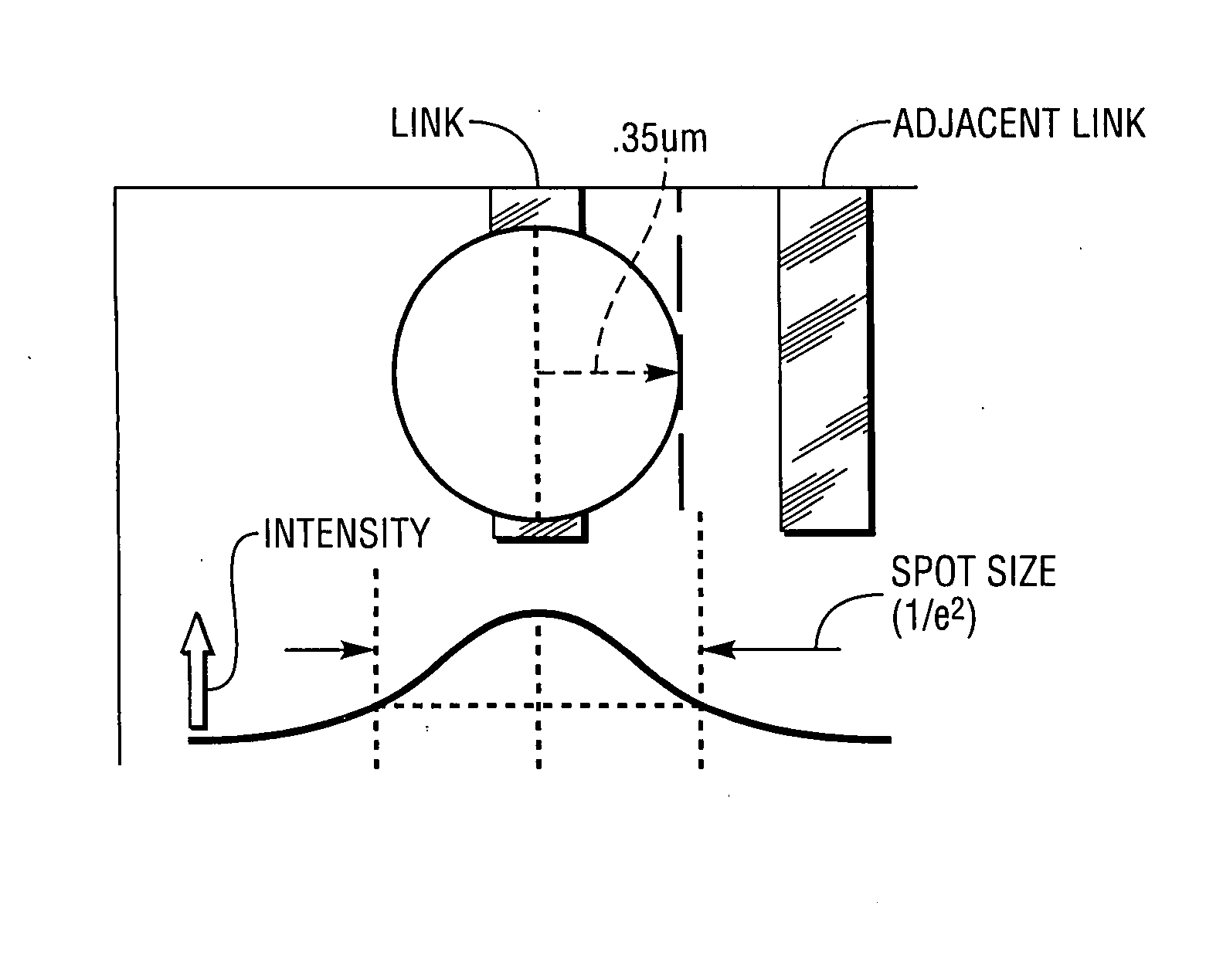
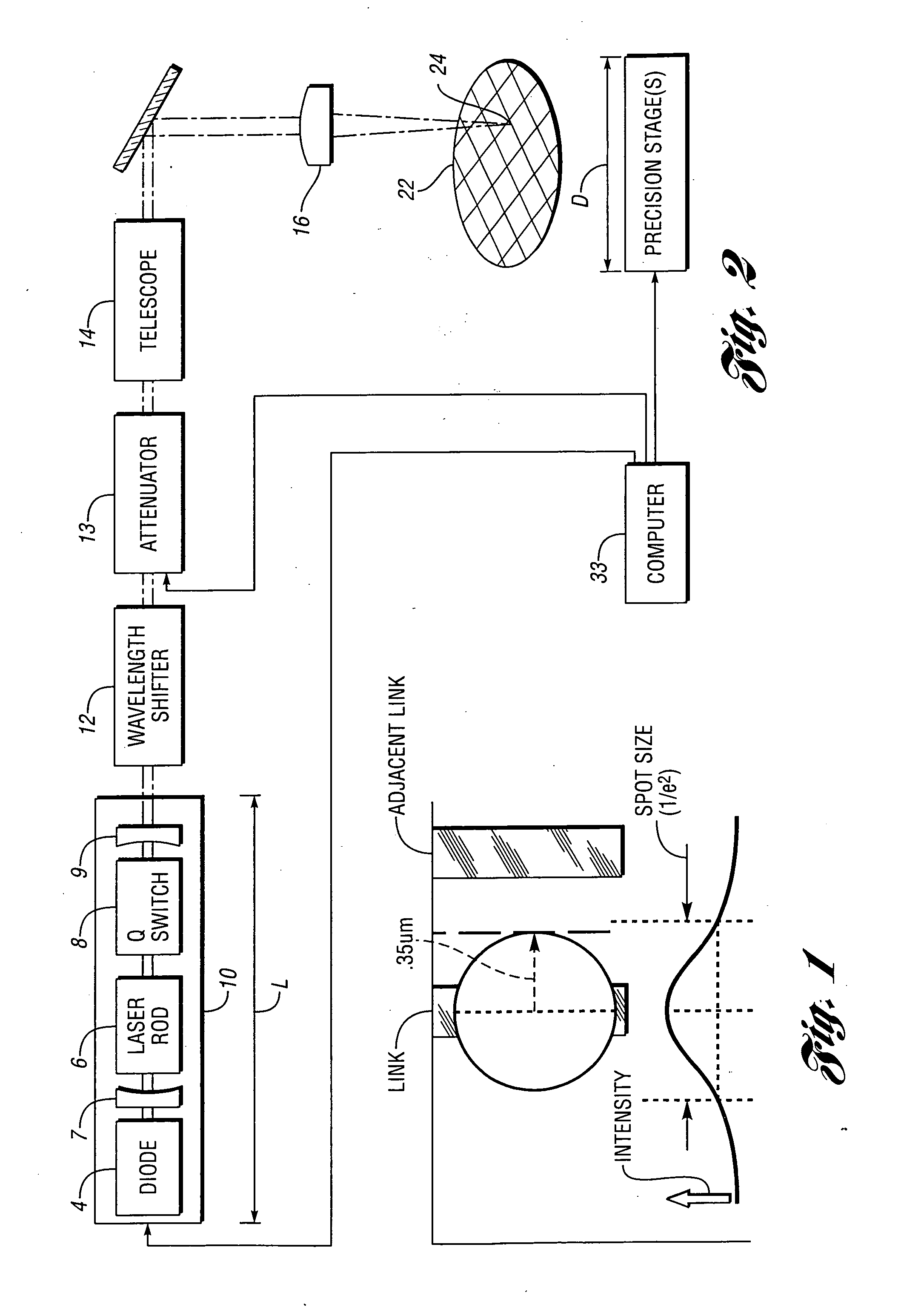
[0069]FIG. 1 (not to scale) illustrates typical dimensions of a target link structure, and an exemplary laser spot used for processing the link structure in accordance with an embodiment of the present invention. The dimensions are representative of very-fine pitch link groups. The target link structure may be separated from the substrate by one or more dielectric layers. The substrate is typically Silicon, but may include other semi-conductive, insulating, or other suitable materials.

[0070] A method and system for processing very fine pitch link structures of a multi-material semiconductor memory device is disclosed. In at least one embodiment the method includes applying at least one laser pulse to a target link structure. The at least one laser pulse has a short wavelength below the absorption edge of the silicon substrate. The at least one laser pulse provides sufficient energy density over a spot size small enough to cleanly remove the link and avoid unacceptable damage to nei...


PUM

PropertyMeasurementUnit
diameteraaaaaaaaaa
diameteraaaaaaaaaa
diameteraaaaaaaaaa

Abstract

A laser-based method and system for selectively processing a multi-material device having a target link structure formed on a substrate while avoiding undesirable change to an adjacent link structure also formed on the substrate are disclosed. The method includes applying at least one focused laser pulse having a wavelength into a spot. The at least one focused laser pulse has an energy density over the spot sufficient to completely process the target link structure while avoiding undesirable change to the adjacent link structure, the substrate and any layers between the substrate and the link structures. The target link structure and the adjacent structure may have a pitch of about 2.0 microns or less.

Description

CROSS-REFERENCE TO RELATED APPLICATIONS AND PATENTS [0001] This application claims the benefit of U.S. provisional application Ser. No. 60 / 765,291, filed Feb. 3, 2006. This application is a continuation-in-part of U.S. Ser. No. 11 / 441,763, filed May 26, 2006. That application is a continuation application of U.S. Ser. No. 11 / 125,367, filed May 9, 2005, which, in turn, is a divisional application of the application which resulted in U.S. Pat. No. 6,972,268, which claims the benefit of U.S. provisional application Ser. No. 60 / 279,644, filed Mar. 29, 2001. This application is related to U.S. Ser. No. 11 / 130,232, filed May 17, 2005 which, in turn, is a continuation application of the application which resulted in U.S. Pat. No. 6,911,622 which, in turn, is a continuation which resulted in U.S. Pat. No. 6,559,412 which, in turn, is a continuation of the application which resulted in U.S. Pat. No. 6,300,590. [0002] The following U.S. patents are hereby incorporated by reference in their en...

Claims


Application Information

Patent Timeline
Patent Type & Authority Applications(United States)
IPC IPC(8): H01L21/00
CPCB23K26/4075H01L27/1052H01L23/5258H01L2924/0002B23K26/40B23K2103/50H10B99/00H01L2924/00
Inventor LEE, JOOHANCORDINGLEY, JAMES J.GU, BOEHRMANN, JONATHAN S.GRIFFITHS, JOSEPH J.
Owner THE GSI GRP LLC
Why Eureka
Try Eureka