Method for Manufacturing Simox Wafer

a manufacturing method and technology of simox, applied in the direction of semiconductor/solid-state device manufacturing, basic electric elements, electric apparatus, etc., can solve the problems of long implantation time, poor manufacturing efficiency, leak current or deterioration in heterointerface, etc., and achieve the effect of not reducing productivity or deterioration in quality

Inactive Publication Date: 2007-08-02
SUMCO CORP
View PDF5 Cites 12 Cited by
  • Summary
  • Abstract
  • Description
  • Claims
  • Application Information

AI Technical Summary

Benefits of technology

[0017]An object of the present invention is to provide a method for manufacturing a SIMOX wafer having a BOX layer with a thin film thickness without a reduction in productivity or deterioration in quality.
[0020]According to the method defined in claim 1, since a gas containing chlorine that is not lower than 0.1 volume % but less than 1.0 volume % is mixed into the atmosphere at the time of temperature elevation in the high-temperature heat treatment, a SIMOX wafer having the BOX layer 15 with a thin film thickness can be manufactured without a reduction in productivity or deterioration in quality.

Problems solved by technology

However, since in this high-dose technology for manufacturing the SIMOX wafer an oxygen ion dose amount is large, there has been a problem that many threading dislocations occur in the SOI layer, an ion implantation time is long and a manufacturing efficiency is poor, for example.
This threading dislocation brings a leak current or deterioration in a heterointerface when a device is manufactured.
As a result, an improvement in device performance or development of functionality may be obstructed.
However, since in this low-dose technology for manufacturing the SIMOX wafer an oxygen ion dose amount is small, a film thickness of the BOX layer becomes thin resulting in a problem of reliability of the BOX layer.
There has been a problem that a percentage of this pin hole density is higher than that of a high-dose SIMOX wafer, for example.
However, even in this ITOX technology manufacturing SIMOX wafer, since an oxygen ion dose amount is large, an ion implantation time is long.
Moreover, a high-temperature oxidizing treatment is required in addition to the annealing treatment, and hence there is a problem that the manufacturing efficiency is poor and the productivity is lowered.
Therefore, re-crystallization of the second ion-implanted layer does not smoothly advance at the time of increasing a temperature in the inert atmosphere, and the second ion-implanted layer becomes a high-density defective layer including polycrystal, a twin crystal, or a stacking fault.
However, in the manufacturing method disclosed in U.S. Pat. No. 5,930,643, oxygen in the oxidizing atmosphere during the high-temperature oxidizing treatment is apt to be precipitated in the high-density defective layer, and a SIMOX wafer having a BOX layer with a thin film thickness demanded by a semiconductor device manufacturer is hard to be manufactured.
However, considering performance of a current anneal furnace, when a high-temperature treatment is carried out at a temperature exceeding 1350° C., a high-quality SIMOX wafer is hard to be manufactured.
Moreover, when an oxygen concentration in the oxidizing atmosphere is lowered, an oxidizing treatment time becomes longer in order to obtain an SOI layer having a predetermined film thickness, resulting in a problem that a manufacturing efficiency is deteriorated and productivity is decreased.

Method used


Image

  • Method for Manufacturing Simox Wafer
  • Method for Manufacturing Simox Wafer
  • Method for Manufacturing Simox Wafer

Examples


example 1

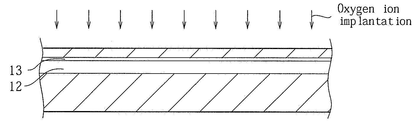
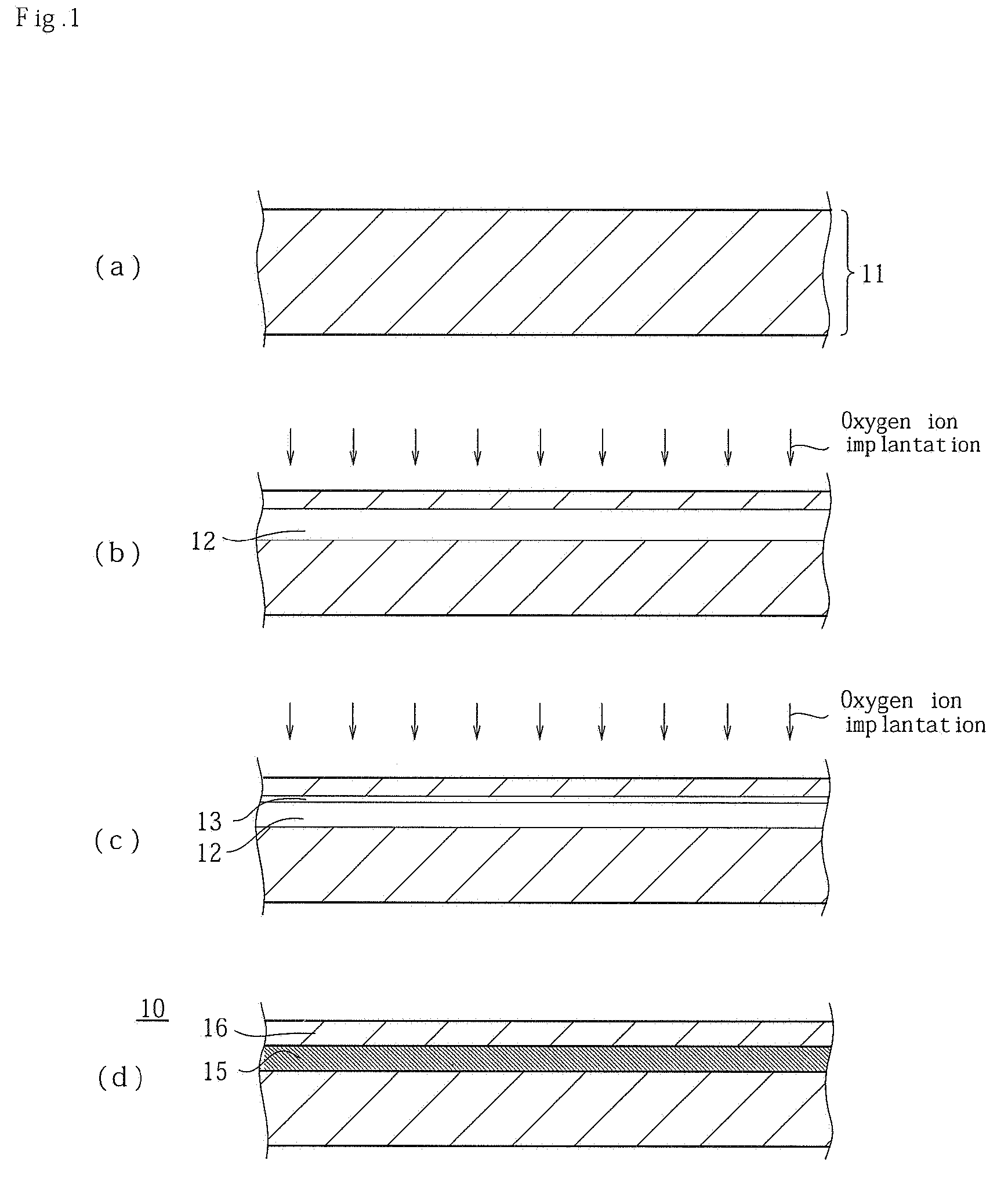
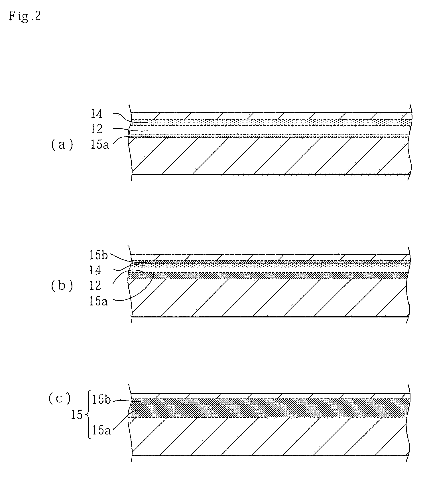
[0047]As shown in FIG. 1, a silicon wafer 11 formed of a P-type silicon wafer having a diameter of 200 mm, a crystal orientation of , and a specific resistance of 10 to 20 Ωcm was first prepared. Then, after accommodating the wafer 11 in the ion implanter, the inside of the implanter was changed to a vacuum state, and a temperature in the implanter was increased to 400° C. Subsequently, oxygen ions (O+) were implanted from a surface of the wafer 11 in a dose amount of 2.4×10¹⁷ atoms / cm2 with an implantation energy of 210 keV to form a first ion-implanted layer 12 in the silicon wafer 11.

[0048]Then, the inside of the implanter was cooled to a room temperature, and the oxygen inos (O+) were implanted from the surface of the silicon wafer 11 in dose amount of 2.0×10¹⁵ atoms / cm2 with the implantation energy of 210 keV to form a second ion-implanted layer 13 in such a manner that the second ion-implanted layer 13 partially overlaps the first ion-implanted layer 12 on a front surface side...

example 2

[0052]A SIMOX wafer 10 was obtained like Example 1 except that the implantation energy at the first ion-implanted layer forming step was changed to 160 keV, the dose amount of the oxygen ions were changed to 2.5×10¹⁷ atoms / cm2, the implantation energy at the second ion-implanted layer forming step was changed to 160 keV, and the dose amount of the oxygen ions were change to 1.5×10¹⁵ atoms / cm2. This SIMOX wafer 10 was determined as Example 2.


PUM

PropertyMeasurementUnit
temperatureaaaaaaaaaa

Abstract

A SIMOX wafer having a BOX layer with a thin film thickness is obtained without a reduction in productivity or deterioration in quality. In a method for manufacturing a SIMOX wafer comprising: a step of forming a first ion-implanted layer in a silicon wafer; a step of forming a second ion-implanted layer that is in an amorphous state; and a high-temperature heat treatment step of maintaining the wafer in an oxygen contained atmosphere at a temperature that is not lower than 1300° C. but less than a silicon melting point for 6 to 36 hours to change the first and the second ion-implanted layers into a BOX layer, a gas containing chlorine that is not less than 0.1 volume % but less than 1.0 volume % is mixed into an atmosphere during temperature elevation in the high-temperature heat treatment.

Description

BACKGROUND OF THE INVENTION[0001]1. Field of the Invention[0002]The present invention relates to a method for manufacturing a SIMOX (Separation by IMplanted Oxygen) wafer based on a SIMOX technology among methods for manufacturing an SOI (Silicon On Insulator) wafer having a single-crystal silicon layer formed on a silicon single-crystal main body via an oxide film.[0003]2. Description of the Related Art[0004]As conventional methods for manufacturing an SOI wafer, there are known a bonding method for bonding two silicon wafers via an oxide film and a SIMOX method for implanting oxygen (O+) ions from a silicon wafer surface to form an ion-implanted layer serving as an oxygen layer having a high concentration in a region at a predetermined depth in a wafer and applying a heat treatment to this wafer to change the ion-implanted layer into a buried oxide film (which will be referred to as a BOX layer hereinafter). In particular, an SOI wafer manufactured by the SIMOX method is called a ...

Claims


Application Information

Patent Timeline
Patent Type & Authority Applications(United States)
IPC IPC(8): H01L21/425H01L21/31
CPCH01L21/76243
Inventor AOKI, YOSHIROKOMATSU, YUKIONAKAI, TETSUYANAKAMURA, SEIICHI
Owner SUMCO CORP
Why Eureka
Try Eureka