Semiconductor device

Inactive Publication Date: 2007-08-02
SEMICON ENERGY LAB CO LTD
View PDF5 Cites 32 Cited by
  • Summary
  • Abstract
  • Description
  • Claims
  • Application Information

AI Technical Summary

Benefits of technology

[0021]In an IC chip having a function of blocking a side-channel attack, by additionally providing a random number generator and an auxiliary arithmetic unit, time change of physical data which leaks from the IC chip can be made more complex. Therefore, it takes time to obtain inside data from physical data intercepted by the third party, thereby security can be improved. Furthermore, in the IC chip having a function of blocking a side-channel attack, there is no need to remake the IC chip back to a stage of mask design regardless of change of the specification by change of the method of blocking the side-channel attack. Consequently, manufacturing cost can be reduced and manufacturing time can be shortened. Further, there is no concern for a defect of an IC chip remade by changing the mask design.
[

Problems solved by technology

The data reading using a bar code, or the like is, however, disadvantageous in that a bar code reader is required to be in contact with the bar code and the amount of data stored in the bar code cannot be increased very much.
However, there is a method capable of dec

Method used


Image

  • Semiconductor device
  • Semiconductor device
  • Semiconductor device

Examples


embodiment mode 1

[0044]This embodiment mode will describe a device structure and a flow chart for achieving a function of blocking a side-channel attack in the present invention.

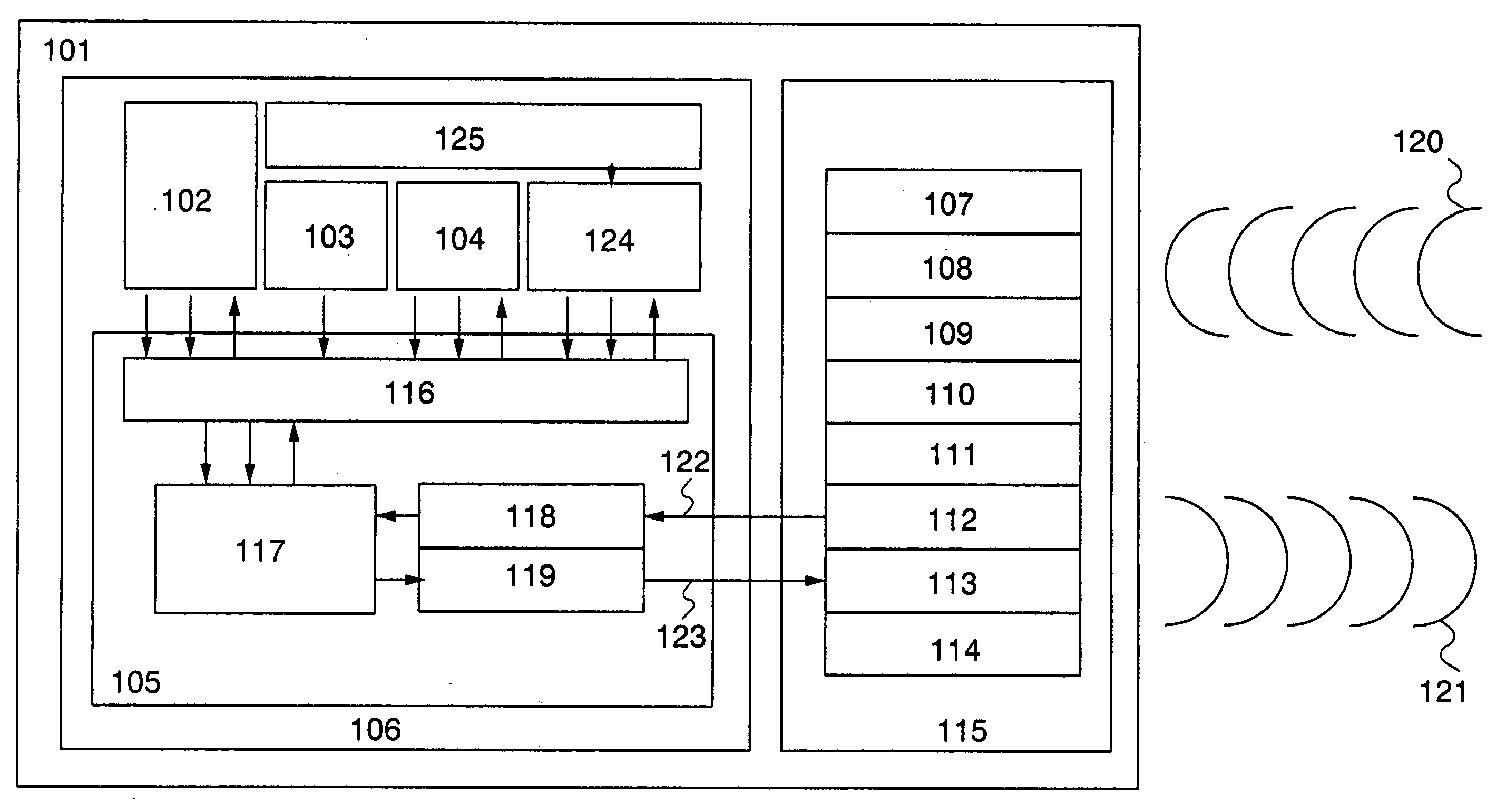
[0045]FIG. 1 is a block diagram of an IC chip for which a function of blocking a side-channel attack in the present invention is provided.

[0046]In FIG. 1, an IC chip 101 includes an arithmetic circuit 106 and an analog portion 115. The arithmetic circuit 106 includes a CPU (also called a Central Processing Unit, or a MPU (microprocessor)) 102, a ROM (also called a Read Only Memory) 103, a RAM (also called a Random Access Memory) 104, an auxiliary arithmetic unit 124, a random number generator 125, and a controller 105. The analog portion 115 includes an antenna 107, a resonant circuit 108, a power supply circuit 109, a reset circuit 110, a clock generating circuit 111, a demodulating circuit 112, a modulating circuit 113, and a power managing circuit 114. The controller 105 includes a CPU interface (CPUIF) 116, a control reg...

embodiment mode 2

[0066]Embodiment Mode 1 shows the structure in which the IC chip can perform the function of blocking a side-channel attack with the side-channel attack blocking program having the plurality of side-channel attack blocking routines, stored in the ROM. This embodiment mode will describe a device structure for realizing a function of blocking a side-channel attack, which is different from Embodiment Mode 1. Since a flow chart in this embodiment mode is similar to that of Embodiment Mode 1, description will be made using the drawings in Embodiment Mode 1 as needed.

[0067]FIG. 12 is a block diagram of an IC chip for which a function of blocking a side-channel attack in the present invention is provided. FIG. 12 is a block diagram in which the auxiliary arithmetic unit 124 is removed from the block diagram of the IC chip of FIG. 1 in Embodiment Mode 1, and which includes, similarly to FIG. 1, the arithmetic circuit 106 including the CPU 102, the ROM 103, the RAM 104, and the random number...

embodiment mode 3

[0075]This embodiment mode will describe a mode of forming an IC chip by using a thin film transistor formed over an insulating substrate.

[0076]As shown in FIG. 13A, an insulating substrate 1300 is prepared. A glass substrate, a quartz substrate, a plastic substrate, or the like can be used as the insulating substrate 1300. Further, these substrates can be made thinner by, for example, polishing their back surfaces. Alternatively, a substrate formed by forming a layer using an insulating material on a conductive substrate formed of a metal element or the like or a semiconductor substrate formed of silicon or the like can be used. For example, by forming an IC chip over a plastic substrate, a highly flexible, lightweight, and thin device can be manufactured.

[0077]A peeling layer 1301 is selectively formed over the insulating substrate 1300. Needless to say, the peeling layer 1301 may be formed over the entire surface of the insulating substrate 1300. The peeling layer 1301 is formed ...


PUM


Abstract

To make it difficult to obtain a secret key from a power change or EM emission intercepted when an IC card encounters a power analysis attack or an electromagnetic wave analysis attack. An arithmetic circuit and a circuit for transmitting/receiving a signal to/from outside are included. The arithmetic circuit includes a central processing unit, an auxiliary arithmetic unit, a random number generator, and a read only memory. The read only memory stores a program for processing of blocking a side-channel attack in signal transmission/reception to/from outside. By additionally providing the random number generator and the auxiliary arithmetic unit, time change of physical data which leaks from an IC chip can be made more complex. This operation is executed by the program. Therefore, it takes time to obtain inside data from physical data intercepted by the third party, thereby security can be improved.

Description

TECHNICAL FIELD[0001]The present invention relates to a semiconductor device. In particular, the present invention relates to a semiconductor device which transmits / receives signals to / from an external device by wireless communication. Note that a semiconductor device here means any device which can function by using semiconductor characteristics. For example, an IC chip for RFID (Radio Frequency Identification) (also called an ID chip, an IC tag, an ID tag, an RF tag, a wireless tag, an electronic tag, or a transponder) is also included in the category of the present invention.BACKGROUND ART[0002]With development of computer technologies and improvement of image recognition technologies, data identification using a medium such as a bar code has widely spread and been used for identification of product data and the like. It is expected that the amount of data to be identified will further increase in the future. The data reading using a bar code, or the like is, however, disadvantag...

Claims


Application Information

Patent Timeline
IPC IPC(8): H04L9/00G06F12/14G06F1/00H04K1/00H04L9/32G06F11/30G06F21/75
CPCG06F21/75H04L2209/805H04L9/0662H04L9/003
Inventor DEMBO, HIROKI
Owner SEMICON ENERGY LAB CO LTD
Why Eureka
Try Eureka